주메뉴
- About IBS 연구원소개
-
Research Centers
연구단소개
- Research Outcomes
- Mathematics
- Physics
- Center for Underground Physics
- Center for Theoretical Physics of the Universe (Particle Theory and Cosmology Group)
- Center for Theoretical Physics of the Universe (Cosmology, Gravity and Astroparticle Physics Group)
- Dark Matter Axion Group
- Center for Artificial Low Dimensional Electronic Systems
- Center for Theoretical Physics of Complex Systems
- Center for Quantum Nanoscience
- Center for Exotic Nuclear Studies
- Center for Van der Waals Quantum Solids
- Center for Relativistic Laser Science
- Chemistry
- Life Sciences
- Earth Science
- Interdisciplinary
- Center for Neuroscience Imaging Research (Neuro Technology Group)
- Center for Neuroscience Imaging Research (Cognitive and Computational Neuroscience Group)
- Center for Algorithmic and Robotized Synthesis
- Center for Genome Engineering
- Center for Nanomedicine
- Center for Biomolecular and Cellular Structure
- Center for 2D Quantum Heterostructures
- Center for Quantum Conversion Research
- Institutes
- Korea Virus Research Institute
- News Center 뉴스 센터
- Career 인재초빙
- Living in Korea IBS School-UST
- IBS School 윤리경영


주메뉴
- About IBS
-
Research Centers
- Research Outcomes
- Mathematics
- Physics
- Center for Underground Physics
- Center for Theoretical Physics of the Universe (Particle Theory and Cosmology Group)
- Center for Theoretical Physics of the Universe (Cosmology, Gravity and Astroparticle Physics Group)
- Dark Matter Axion Group
- Center for Artificial Low Dimensional Electronic Systems
- Center for Theoretical Physics of Complex Systems
- Center for Quantum Nanoscience
- Center for Exotic Nuclear Studies
- Center for Van der Waals Quantum Solids
- Center for Relativistic Laser Science
- Chemistry
- Life Sciences
- Earth Science
- Interdisciplinary
- Center for Neuroscience Imaging Research (Neuro Technology Group)
- Center for Neuroscience Imaging Research (Cognitive and Computational Neuroscience Group)
- Center for Algorithmic and Robotized Synthesis
- Center for Genome Engineering
- Center for Nanomedicine
- Center for Biomolecular and Cellular Structure
- Center for 2D Quantum Heterostructures
- Center for Quantum Conversion Research
- Institutes
- Korea Virus Research Institute
- News Center
- Career
- Living in Korea
- IBS School
News Center
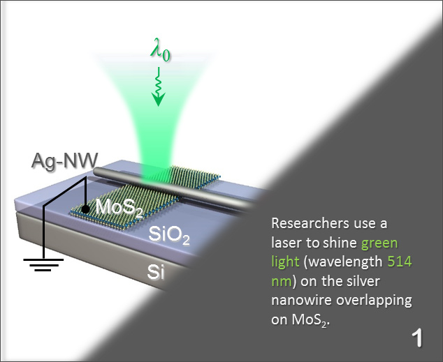
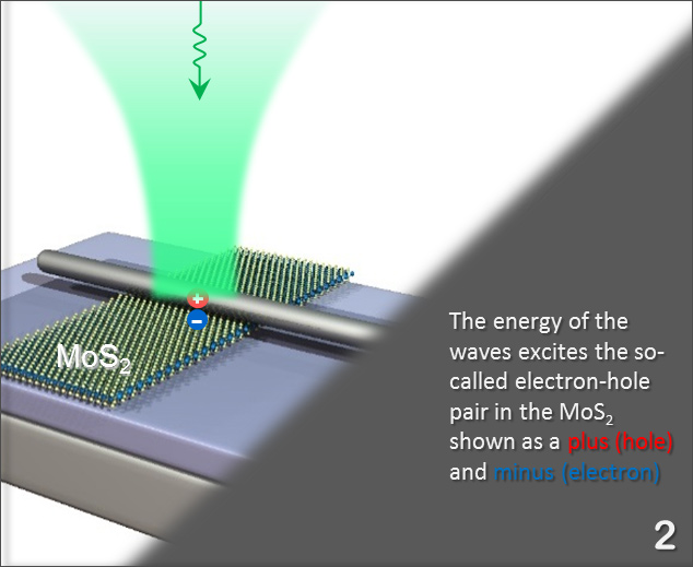
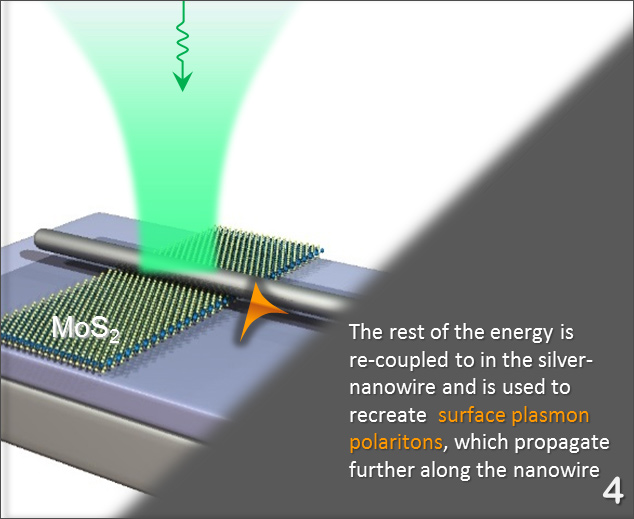
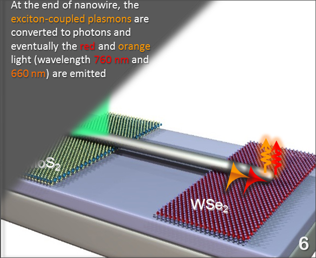
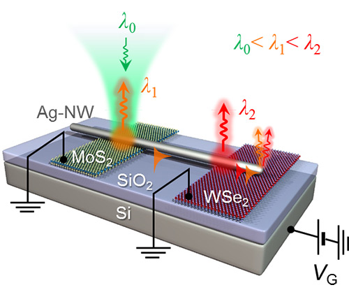
Squeezing Light Into New Miniature Devices- IBS develops new optical circuit components to manipulate light - Do you think your computer is fast enough? Think again. The computers of the future could work almost at the speed of light! Nanophotonics, the study of light at the nanometer scale, could indeed bring the speed of our technology to a completely different level. The Center for Integrated Nanostructure Physics (CINAP) within the Institute for Basic Science (IBS) have developed three key components of a circuit that works with light. Published in Nature Communications, these devices combine the advantages of photonics and electronics on the same platform. While we are slowing approaching the end point of Moore's Law: a state where we physically cannot shrink the dimension of our transistors much further; the future of big data processing requires high performance computers with higher speed operations. Researchers reckon that if we build computers that process information through light, instead of electrons, computers will be able to work faster. However, at nanometer dimensions, the wavelength of light is larger than the diameter of the silicon fiber and for this reason some light can be lost. A solution to control the propagation of light in matter can come from surface plasmons. These are electromagnetic waves that propagate along the surface of some conductive materials like silver, gold, aluminum and copper. Using surface plasmons, optical information can be transmitted nearly at the speed of light and in extremely miniature volumes. Using surface plasmons in silver nanowires and 2D semiconductors like molybdenum disulphide (MoS2), IBS scientists built three key components for optical communication: optical transistors, optical multiplexers and optical signal detectors. These devices work thanks to a phenomenon called plasmon-exciton-plasmon interconversion. The graphics describe the details of this process step-by-step:
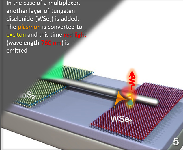
How does light make it through the device? The video explains it step-by-step. IBS scientists constructed the optical transistor by interconnecting the silver nanowire to a flake of MoS2. Light shone on the device is converted to surface plasmon, than to exciton, back to surface plasmon and eventually emitted as light with a shorter wavelength compared to the initial input. For example, if the input light is green, the output light can be red. Wavelength multiplexing devices were realized in a similar way, but instead of having only a flake of MoS2, the researchers used an array of three different 2D semiconductor materials emitting light at different wavelengths. In this structure, for example, a single input light (violet color) generates three output lights (blue, green and red). The propagating optical signals along the silver nanowire can be also transformed and detected as electrical signals by an optical signal detector.
"The originality of this paper arises from the exciton-plasmon interconversion. We published before the conversion of exciton to plasmon, and from plasmon to exciton using silver nanowire/2D semiconductor hybrids, but this is the first time that we can complete the circle going from plasmons to excitons and back to plasmons. Using this concept, we created optical transistors and multiplexers," explains professor Hyun Seok Lee, first author of this study. Letizia Diamante Notes for editors - References - Media Contact - About the Institute for Basic Science (IBS) |
|||
Center for Integrated Nanostructure PhysicsPublication Repository |
|||
|
|
| Next | |
|---|---|
| before |
- Content Manager
- Public Relations Team : Yim Ji Yeob 042-878-8173
- Last Update 2023-11-28 14:20


