


주메뉴
- About IBS 연구원소개
-
Research Centers
연구단소개
- Research Outcomes
- Mathematics
- Physics
- Center for Underground Physics
- Center for Theoretical Physics of the Universe (Particle Theory and Cosmology Group)
- Center for Theoretical Physics of the Universe (Cosmology, Gravity and Astroparticle Physics Group)
- Dark Matter Axion Group
- Center for Artificial Low Dimensional Electronic Systems
- Center for Theoretical Physics of Complex Systems
- Center for Quantum Nanoscience
- Center for Exotic Nuclear Studies
- Center for Van der Waals Quantum Solids
- Center for Relativistic Laser Science
- Chemistry
- Life Sciences
- Earth Science
- Interdisciplinary
- Center for Neuroscience Imaging Research (Neuro Technology Group)
- Center for Neuroscience Imaging Research (Cognitive and Computational Neuroscience Group)
- Center for Algorithmic and Robotized Synthesis
- Center for Genome Engineering
- Center for Nanomedicine
- Center for Biomolecular and Cellular Structure
- Center for 2D Quantum Heterostructures
- Center for Quantum Conversion Research
- Institutes
- Korea Virus Research Institute
- News Center 뉴스 센터
- Career 인재초빙
- Living in Korea IBS School-UST
- IBS School 윤리경영

주메뉴
- About IBS
-
Research Centers
- Research Outcomes
- Mathematics
- Physics
- Center for Underground Physics
- Center for Theoretical Physics of the Universe (Particle Theory and Cosmology Group)
- Center for Theoretical Physics of the Universe (Cosmology, Gravity and Astroparticle Physics Group)
- Dark Matter Axion Group
- Center for Artificial Low Dimensional Electronic Systems
- Center for Theoretical Physics of Complex Systems
- Center for Quantum Nanoscience
- Center for Exotic Nuclear Studies
- Center for Van der Waals Quantum Solids
- Center for Relativistic Laser Science
- Chemistry
- Life Sciences
- Earth Science
- Interdisciplinary
- Center for Neuroscience Imaging Research (Neuro Technology Group)
- Center for Neuroscience Imaging Research (Cognitive and Computational Neuroscience Group)
- Center for Algorithmic and Robotized Synthesis
- Center for Genome Engineering
- Center for Nanomedicine
- Center for Biomolecular and Cellular Structure
- Center for 2D Quantum Heterostructures
- Center for Quantum Conversion Research
- Institutes
- Korea Virus Research Institute
- News Center
- Career
- Living in Korea
- IBS School


News Center

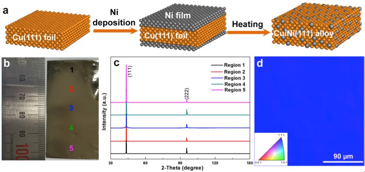
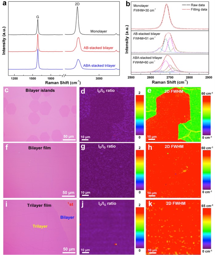
Well-designed substrates make large single crystal bi-/tri-layer graphene possible- IBS researchers fabricate single crystal copper nickel alloy foils as substrates for the growth of multilayer graphene with specific stacking pattern, and unprecedented quality and size - Researchers of the Center for Multidimensional Carbon Materials (CMCM) within the Institute for Basic Science (IBS, South Korea) have reported in Nature Nanotechnology the fabrication and use of single crystal copper-nickel alloy foil substrates for the growth of large-area, single crystal bilayer and trilayer graphene films. The growth of large area graphene films with a precisely controlled numbers of layers and stacking orders can open new possibilities in electronics and photonics but remains a challenge. This study showed the first example of the synthesis of bi- and trilayer graphene sheets larger than a centimeter, with layers piled up in a specific manner, namely AB- and ABA-stacking. “This work provides materials for the fabrication of graphene devices with novel functions that have not yet been realized and might afford new photonic and optoelectronic and other properties,” explains Rodney S. Ruoff, CMCM Director, Distinguished Professor at the Ulsan National Institute of Science and Technology (UNIST) and leading author of this study. Coauthor and Professor Won Jong Yoo of Sungkyunkwan University notes that “this paves the way for the study of novel electrical transport properties of bilayer and trilayer graphene.” For example, the same IBS research group and collaborators recently published another paper in Nature Nanotechnology showing the conversion of AB-stacked bilayer graphene film, grown on copper/nickel (111) alloy foils (Cu/Ni(111) foils), to a diamond-like sheet, known as diamane. Coauthor Pavel V. Bakharev notes that: “Less than one year ago, we produced fluorinated diamond monolayer, F-diamane, by fluorination of exactly the AB-stacked bilayer graphene films described in this new paper. Now the possibility of producing bilayer graphene of a larger size brings renewed excitement and shows how fast this field is developing.” The right choice of substrate is essential for the correct growth of graphene. Foils made only of copper limit the growth of bilayer graphene and favor uniform monolayer growth. It is possible to obtain multilayer graphene sheets on nickel film, but these are not uniform, and tend to have small “patches” with different thicknesses. Finally, the commercially available foils that contain both nickel and copper are not ideal. Therefore, IBS researchers prepared ‘home-made’ single crystal Cu/Ni(111) foils with desired features, building further on a technique reported by the group in Science in 2018. Nickel films are electroplated onto copper(111)-foils so that the nickel and copper interdiffuse when heated and yield a new single crystal foil that contains both elements at adjustable ratios. Ruoff suggested this method and supervised Ming Huang’s evaluations of the best concentrations of nickel to obtain uniform graphene sheets with the desired number of layers.
IBS researchers grew bi- and tri-layer graphene sheets on Cu/Ni(111) foils by chemical vapor deposition (CVD). Huang achieved AB-stacked bilayer graphene films of several square centimeters, covering 95% of the substrate area, and ABA-stacked trilayer graphene with more than 60% areal coverage. This represents the first growth of high coverage ABA-stacked trilayer graphene over a large area and the best quality obtained for AB-stacked bilayer graphene so far. In addition to extensive spectroscopic and microscopic characterizations, the researchers also measured the electrical transport (carrier mobility and band gap tunability) and thermal conductivity of the newly synthesized graphene. The centimeter-scale bilayer graphene films showed a good thermal conductivity, as high as ~2300 W/mK (comparable with exfoliated bilayer graphene flakes), and mechanical performance (stiffness of 478 gigapascals for the Young’s modulus, and 3.31 gigapascals for the fracture strength). The team then investigated the growth stacking mechanism and discovered it follows the so-called “inverted wedding cake” sequence as the bottom layers are positioned after the top one. “We showed with three independent methods that the 2nd layer for bilayer graphene, and the 2nd and 3rd layers of the trilayer sheet grow beneath a continuous top layer. These methods can be further used to study the structure and stacking sequence of other 2D thin film materials,” notes Huang. Ruoff notes that these techniques for synthesizing and testing large-scale ultrathin films could stimulate worldwide interest in further experimenting with single crystal Cu/Ni alloy foils, and even in exploring fabrication and use of other single crystal alloy foils. This research was performed in collaboration with UNIST and Sungkyunkwan University.
Notes for editors - References - Media Contact - About the Institute for Basic Science (IBS) |
|||
|
|
| Next | |
|---|---|
| before |
- Content Manager
- Public Relations Team : Yim Ji Yeob 042-878-8173
- Last Update 2023-11-28 14:20
55, Expo-ro, Yuseong-gu, Daejeon, Korea, 34126
Tel. +82-42-878-8114 | Fax. +82-42-878-8079 | E-mail. webmaster@ibs.re.kr
Copyright(c) IBS. All Rights Reserved.
