


주메뉴
- About IBS 연구원소개
-
Research Centers
연구단소개
- Research Outcomes
- Mathematics
- Physics
- Center for Underground Physics
- Center for Theoretical Physics of the Universe (Particle Theory and Cosmology Group)
- Center for Theoretical Physics of the Universe (Cosmology, Gravity and Astroparticle Physics Group)
- Dark Matter Axion Group
- Center for Artificial Low Dimensional Electronic Systems
- Center for Quantum Nanoscience
- Center for Exotic Nuclear Studies
- Center for Van der Waals Quantum Solids
- Center for Relativistic Laser Science
- Center for Trapped Ion Quantum Science
- Chemistry
- Life Sciences
- Center for Memory and Glioscience (Cognitive Glioscience Group)
- Center for Memory and Glioscience (Learning and Memory Group)
- Center for Synaptic Brain Dysfunctions
- Center for RNA Research
- Center for Genomic Integrity
- Center for Vascular Research
- Center for Genome Engineering
- Center for Microbiome–Body–Brain Physiology
- Earth Science
- Interdisciplinary
- Center for Neuroscience Imaging Research (Neuro Technology Group)
- Center for Neuroscience Imaging Research (Cognitive and Computational Neuroscience Group)
- Center for Algorithmic and Robotized Synthesis
- Center for Nanomedicine
- Center for Biomolecular and Cellular Structure
- Center for 2D Quantum Heterostructures
- Institutes
- Korea Virus Research Institute
- News Center 뉴스 센터
- Career 인재초빙
- Living in Korea IBS School-UST
- IBS School 윤리경영

주메뉴
- About IBS
-
Research Centers
- Research Outcomes
- Mathematics
- Physics
- Center for Underground Physics
- Center for Theoretical Physics of the Universe (Particle Theory and Cosmology Group)
- Center for Theoretical Physics of the Universe (Cosmology, Gravity and Astroparticle Physics Group)
- Dark Matter Axion Group
- Center for Artificial Low Dimensional Electronic Systems
- Center for Quantum Nanoscience
- Center for Exotic Nuclear Studies
- Center for Van der Waals Quantum Solids
- Center for Relativistic Laser Science
- Center for Trapped Ion Quantum Science
- Chemistry
- Life Sciences
- Center for Memory and Glioscience (Cognitive Glioscience Group)
- Center for Memory and Glioscience (Learning and Memory Group)
- Center for Synaptic Brain Dysfunctions
- Center for RNA Research
- Center for Genomic Integrity
- Center for Vascular Research
- Center for Genome Engineering
- Center for Microbiome–Body–Brain Physiology
- Earth Science
- Interdisciplinary
- Center for Neuroscience Imaging Research (Neuro Technology Group)
- Center for Neuroscience Imaging Research (Cognitive and Computational Neuroscience Group)
- Center for Algorithmic and Robotized Synthesis
- Center for Nanomedicine
- Center for Biomolecular and Cellular Structure
- Center for 2D Quantum Heterostructures
- Institutes
- Korea Virus Research Institute
- News Center
- Career
- Living in Korea
- IBS School


News Center

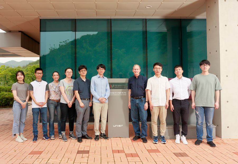
Graphenes now go monolayer and single crystalline- The high-performance device is fabricated in “clean areas” in between graphene folds - Director Rodney Ruoff’s research group from the Center for Multidimensional Carbon Materials (CMCM) within the Institute for Basic Science (IBS) at the Ulsan National Institute of Science and Technology (UNIST) has reported a truly single layer (i.e., adlayer-free) large area graphene film on large area copper foils. This might seem like the latest in a series of seemingly similar declarations on single layer graphene. However, this achievement differs from other thousands of previous publications in that none of them had described truly single layer graphene over large area. Adlayers (bilayer or multilayer regions) have always been present in such films.
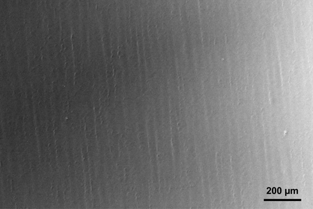
IBS scientists refined the chemical vapor deposition (CVD) growth method by eliminating all carbon impurities inside the copper foils on which graphene is grown. CVD on metal foils (especially copper foils) is currently the most promising route for scalable and reproducible synthesis of large-area graphene films of high quality. The team investigated why “adlayers” appeared in the graphene film grown on copper foils and found that the carbon impurities inside the foil directly lead to the nucleation and growth of adlayers. (Adlayers are regions in the film where there are 2 layers or 3 layers present—multilayer “patches”, that is.) “We discovered that the commercial copper foils have ‘excess carbon’ particularly near the surface—to a depth of about 300 nm, by using time-of-flight secondary ion mass spectrometry and combustion analysis. From a discussion with one technical expert in Jiangxi Copper Corporation Limited, one of the world’s largest suppliers of copper foils, we learned that the carbon is embedded in the copper foil during manufacture, probably from hydrocarbon-based oil(s) used to lubricate rollers that the copper foil contacts at the high rolling temperatures”, said Dr. Da Luo, first author of the article. After completely removing this carbon by annealing under H2 at 1060 °C, they were able to achieve adlayer-free and thus truly single layer graphene film.
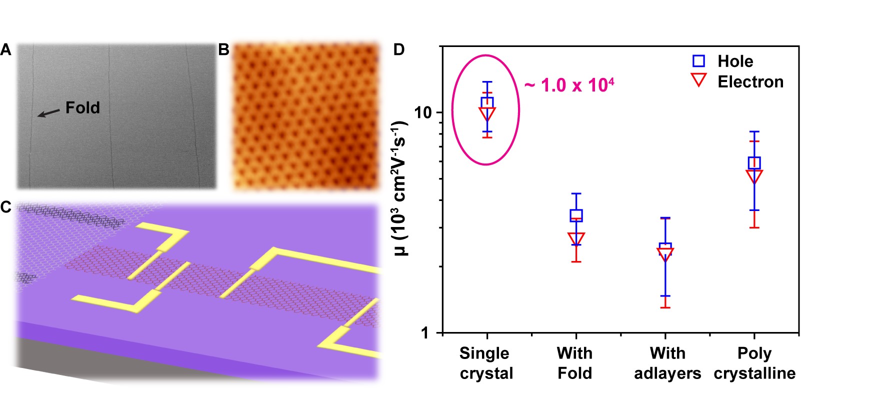
By applying the same method, the IBS scientists also obtained an adlayer-free single layer and single crystal graphene film on a single crystal Cu foil. One of the first authors Meihui Wang explained, “We thus solved two problems that have persistently been present in prior syntheses of CVD graphene films (adlayers and grain boundaries (GBs)) at one time.” Indeed, achieving perfect uniformity in the number of layers over a large area (single or double layers, for example) can be used to ensure a consistent device performance. Adlayer regions differ in, e.g., density and size when present in the active regions of devices. In addition to adlayers, GBs are present in polycrystalline graphene films prepared by CVD where graphene islands with different crystallographic orientations join to complete the film. The presence of GBs lowers carrier mobility and thermal conductivity, and reduces the mechanical strength.
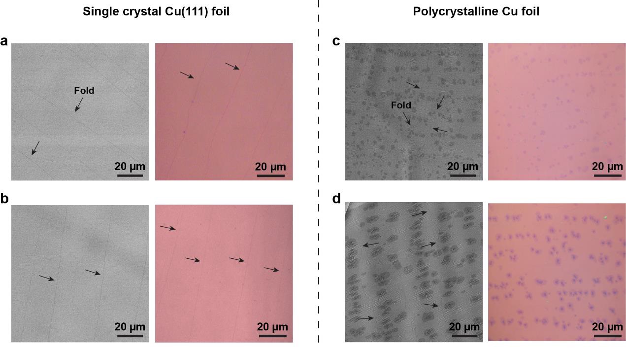
Still, the scientists were left with one fascinating feature in their single crystal films: This single crystal graphene contains highly oriented parallel “folds” that are centimeters in length, roughly a hundred nanometers in width, and separated by 20 to 50 micrometers. Just like adlayers and GBs, folds were observed to significantly decrease the carrier mobility of graphene. To eliminate such scattering effects of adlayers, GBs and folds, the team patterned field-effect transistors in the region lying between two adjacent folds and with the transistors parallel to the folds. Unlike folds distributed quasi-randomly in the polycrystalline graphene film, the folds are highly aligned in the large area single crystal graphene film. This makes it easy to fabricate integrated high performance devices from the regions between the folds. Wang explained, “The region between two adjacent folds is ‘clean’ without any folds, adlayers, or GBs. This enabled the device to have very high electron and hole mobility. The field-effect transistors show very high room temperature carrier mobility values of around 1.0 x 104 cm2V-1s-1. Such high carrier mobility “translates” to various useful devices having high performance.”
Director Ruoff noted, “Our approach towards large area adlayer-free single crystal graphene is a breakthrough. This uniform, ‘perfect’ single layer, single crystal graphene is expected to find use as an ultrathin support material for high-resolution transmission electron microscopy imaging, and in optical devices. Also as an appropriate graphene to achieve extremely uniform functionalization which leads to many other applications, particularly for sensors of various types. I also would like to note that we greatly valued the strong contributions by coauthors from UNIST, from HKUST, and from SKKU.” This research was supported by the Institute for Basic Science, and has been published in the journal Advanced Materials. Dahee Carol Kim Notes for editors - References - Media Contact - About the Institute for Basic Science (IBS) |
|||
Center for Multidimensional Carbon MaterialsPublication Repository |
|||
|
|

| Next | |
|---|---|
| before |
- Content Manager
- Public Relations Team : Suh, William Insang 042-878-8137
- Last Update 2023-11-28 14:20
55, Expo-ro, Yuseong-gu, Daejeon, Korea, 34126
Tel. +82-42-878-8114 | Fax. +82-42-878-8079 | E-mail. webmaster@ibs.re.kr
Copyright(c) IBS. All Rights Reserved.
