


주메뉴
- About IBS 연구원소개
-
Research Centers
연구단소개
- Research Outcomes
- Mathematics
- Physics
- Center for Underground Physics
- Center for Theoretical Physics of the Universe (Particle Theory and Cosmology Group)
- Center for Theoretical Physics of the Universe (Cosmology, Gravity and Astroparticle Physics Group)
- Dark Matter Axion Group
- Center for Artificial Low Dimensional Electronic Systems
- Center for Theoretical Physics of Complex Systems
- Center for Quantum Nanoscience
- Center for Exotic Nuclear Studies
- Center for Van der Waals Quantum Solids
- Center for Relativistic Laser Science
- Chemistry
- Life Sciences
- Earth Science
- Interdisciplinary
- Center for Neuroscience Imaging Research (Neuro Technology Group)
- Center for Neuroscience Imaging Research (Cognitive and Computational Neuroscience Group)
- Center for Algorithmic and Robotized Synthesis
- Center for Genome Engineering
- Center for Nanomedicine
- Center for Biomolecular and Cellular Structure
- Center for 2D Quantum Heterostructures
- Center for Quantum Conversion Research
- Institutes
- Korea Virus Research Institute
- News Center 뉴스 센터
- Career 인재초빙
- Living in Korea IBS School-UST
- IBS School 윤리경영

주메뉴
- About IBS
-
Research Centers
- Research Outcomes
- Mathematics
- Physics
- Center for Underground Physics
- Center for Theoretical Physics of the Universe (Particle Theory and Cosmology Group)
- Center for Theoretical Physics of the Universe (Cosmology, Gravity and Astroparticle Physics Group)
- Dark Matter Axion Group
- Center for Artificial Low Dimensional Electronic Systems
- Center for Theoretical Physics of Complex Systems
- Center for Quantum Nanoscience
- Center for Exotic Nuclear Studies
- Center for Van der Waals Quantum Solids
- Center for Relativistic Laser Science
- Chemistry
- Life Sciences
- Earth Science
- Interdisciplinary
- Center for Neuroscience Imaging Research (Neuro Technology Group)
- Center for Neuroscience Imaging Research (Cognitive and Computational Neuroscience Group)
- Center for Algorithmic and Robotized Synthesis
- Center for Genome Engineering
- Center for Nanomedicine
- Center for Biomolecular and Cellular Structure
- Center for 2D Quantum Heterostructures
- Center for Quantum Conversion Research
- Institutes
- Korea Virus Research Institute
- News Center
- Career
- Living in Korea
- IBS School


News Center

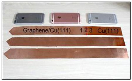
Large Single-Crystal Graphene is Possible!- The target of large, cheap and quick graphene synthesis achieved: 5 x 50 cm2 and beyond - Boasting the conductivity, strength and flexibility we wished for, graphene was proposed as one of the most likely substitutes for silicon and other materials. Its launch into the market however is still slow. What is curbing graphene from industrial applications? One factor is that top quality single-crystal graphene produced so far is just a couple of millimeters or maximum centimeters in size. Recently, a team led by Prof. Feng Ding and Prof. Rodney Ruoff at the Center for Multidimensional Carbon Materials within the Institute for Basic Science (IBS), Prof. Kaihui Liu at Peking University, and their collaborators reported the synthesis of a large sheet of monolayer single-crystal graphene. This result allows a leap forward in graphene production: advancing from a technique that synthesizes a few cm2 sheet of single-crystal graphene in a couple of hours, to an optimized method that allows the creation of an almost-perfect (> 99.9 % aligned) 5 × 50 cm2 single-crystal graphene in just 20 minutes. Moreover, the low production costs, comparable to commercially available lower quality polycrystalline graphene films, could expand its usability. Detailed in Science Bulletin, the method is expected to stimulate further fundamental work on graphene and related materials, including large scale folding of graphene sheets, similar to paper, creating origami-like or kirigami-like shapes, which could be applied to future flexible circuits.
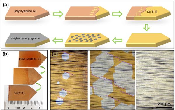
A honeycomb-shaped monolayer of carbon atoms, uniform throughout the whole material, offers its exceptional properties to single-crystal graphene. On the other hand, polycrystalline graphene is formed by randomly oriented graphene islands, which decrease its quality. Currently, scientists are able to grow meter-sized polycrystalline graphene and smaller single-crystal graphene, ranging from 0.01 mm2 to a few cm2. The synthesis of large single-crystal graphene at a low cost has been considered a critical goal of graphene synthesis. In this study, graphene is grown on the surface of a 5 × 50 cm2 copper foil, which was transformed into a single-crystal copper foil by heating to ~ 1,030℃. A temperature slope from hot to cold moved the so-called grain boundary onwards, creating a perfect single-crystal. In the heating and cooling treatment, copper atoms migrate inside the material, arranging into an ordered structure with fewer defects. "The secret to obtain single-crystal graphene of very large size, is to have a perfect single crystal copper as a base to start with. Large single-crystal copper foil is not available in the market, so labs must build it with their own means," explains Feng Ding, group leader at the Center for Multidimensional Carbon Materials. Then, with another technique called chemical vapor deposition, millions of parallel graphene islands are formed on the copper foil surface. As more carbon atoms deposit on the foil, the islands keep on growing until they coalesce and form a very-close-to-perfect single-crystal graphene layer that covering the entire available surface.
In order to optimize the technique, the team had to consider four technical challenges: (i) preparation of single-crystal copper foil in a very large area, (ii) obtaining a high degree of alignment of the graphene islands following their nucleation and growth, (iii) seamlessly stitching the graphene islands into a single crystal through further growth and (iv) the fast growth of single-crystal graphene. Although previous reports have addressed some of the above challenges, this study overcame all of them and made the synthesis of meter-sized single-crystal graphene possible. The degree of the misaligned graphene islands is less than 0.1%, thus great reduced defects and grain boundaries in the products. The current result was limited only by the size of the copper foil and, in principle, both the size of the copper foil and graphene film could perhaps be unlimited. In addition, considering the very short time of graphene synthesis (20 minutes) and the relatively low-cost experimental setup, the price of a single-crystal (or nearly single-crystal) graphene could be close to that of current polycrystalline graphene films. "The dream of many scientists is to make it the material of the future, to replace silicon," enthuses Ding. "Now we are exploring which is the best material to grow graphene on top and how to use copper as a substrate for other interesting 2D materials." Letizia Diamante Notes for editors - References - Media Contact - About the Institute for Basic Science (IBS) |
|||
Center for Multidimensional Carbon MaterialsPublication Repository |
|||
|
|

| before | |
|---|---|
| before |
- Content Manager
- Public Relations Team : Yim Ji Yeob 042-878-8173
- Last Update 2023-11-28 14:20
55, Expo-ro, Yuseong-gu, Daejeon, Korea, 34126
Tel. +82-42-878-8114 | Fax. +82-42-878-8079 | E-mail. webmaster@ibs.re.kr
Copyright(c) IBS. All Rights Reserved.
