


주메뉴
- About IBS 연구원소개
-
Research Centers
연구단소개
- Research Outcomes
- Mathematics
- Physics
- Center for Underground Physics
- Center for Theoretical Physics of the Universe (Particle Theory and Cosmology Group)
- Center for Theoretical Physics of the Universe (Cosmology, Gravity and Astroparticle Physics Group)
- Dark Matter Axion Group
- Center for Artificial Low Dimensional Electronic Systems
- Center for Theoretical Physics of Complex Systems
- Center for Quantum Nanoscience
- Center for Exotic Nuclear Studies
- Center for Van der Waals Quantum Solids
- Center for Relativistic Laser Science
- Chemistry
- Life Sciences
- Earth Science
- Interdisciplinary
- Center for Neuroscience Imaging Research (Neuro Technology Group)
- Center for Neuroscience Imaging Research (Cognitive and Computational Neuroscience Group)
- Center for Algorithmic and Robotized Synthesis
- Center for Genome Engineering
- Center for Nanomedicine
- Center for Biomolecular and Cellular Structure
- Center for 2D Quantum Heterostructures
- Center for Quantum Conversion Research
- Institutes
- Korea Virus Research Institute
- News Center 뉴스 센터
- Career 인재초빙
- Living in Korea IBS School-UST
- IBS School 윤리경영

주메뉴
- About IBS
-
Research Centers
- Research Outcomes
- Mathematics
- Physics
- Center for Underground Physics
- Center for Theoretical Physics of the Universe (Particle Theory and Cosmology Group)
- Center for Theoretical Physics of the Universe (Cosmology, Gravity and Astroparticle Physics Group)
- Dark Matter Axion Group
- Center for Artificial Low Dimensional Electronic Systems
- Center for Theoretical Physics of Complex Systems
- Center for Quantum Nanoscience
- Center for Exotic Nuclear Studies
- Center for Van der Waals Quantum Solids
- Center for Relativistic Laser Science
- Chemistry
- Life Sciences
- Earth Science
- Interdisciplinary
- Center for Neuroscience Imaging Research (Neuro Technology Group)
- Center for Neuroscience Imaging Research (Cognitive and Computational Neuroscience Group)
- Center for Algorithmic and Robotized Synthesis
- Center for Genome Engineering
- Center for Nanomedicine
- Center for Biomolecular and Cellular Structure
- Center for 2D Quantum Heterostructures
- Center for Quantum Conversion Research
- Institutes
- Korea Virus Research Institute
- News Center
- Career
- Living in Korea
- IBS School


News Center

| Title | Highly conductive and elastic nanomembrane for skin electronics | ||
|---|---|---|---|
| Embargo date | 2021-08-27 03:00 | Hits | 2948 |
| Press release | |||
| att. | |||
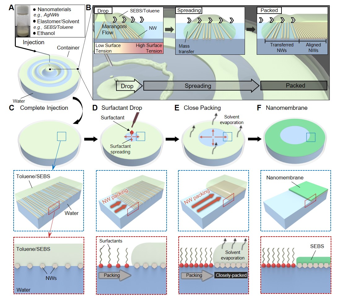
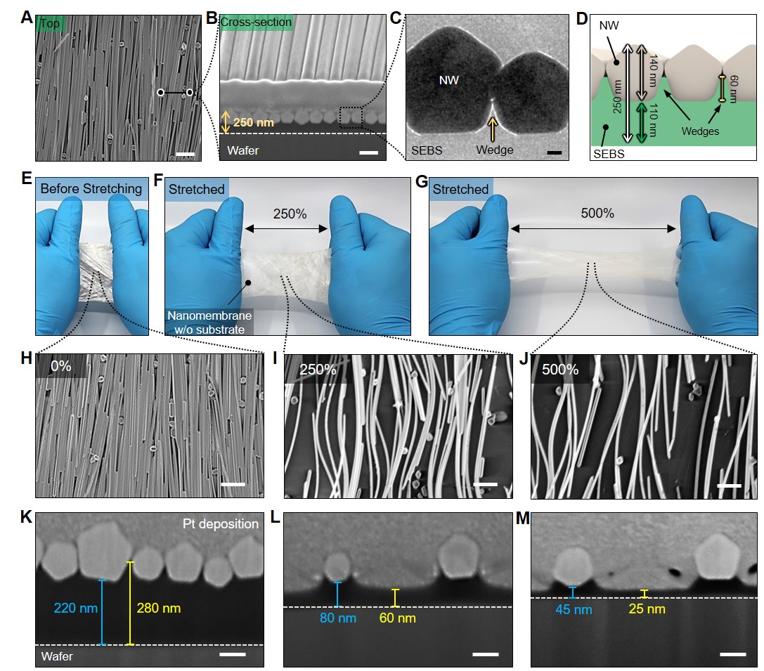
Highly conductive and elastic nanomembrane for skin electronicsA float assembly method enables the fabrication of highly conductive, stretchable, and ultrathin nanomembranes Skin electronics require stretchable conductors that satisfy metal-like conductivity, high stretchability, ultrathin thickness, and ease of patternability, but it is challenging to achieve these characteristics simultaneously. The researchers developed a new float assembly method to fabricate a nanomembrane that satisfies all these requirements simultaneously. The exceptional material properties are attributed to its unique cross-sectional structure in which a monolayer of compactly assembled nanomaterials is partially embedded in an ultrathin elastomer membrane. “Skin electronics” are thin flexible electronics that could be mounted onto the skin. While it may sound like something out of science fiction, it is anticipated that soon such devices can serve as next-generation devices with a wide range of applications such as health monitoring, health diagnosis, virtual reality, and human-machine interface. As it is expected, creating such devices requires components that are soft and stretchable to be mechanically compatible with the human skin. One of the vital components of skin electronics is an intrinsically stretchable conductor that transmits electrical signals between devices. For reliable operation and high-quality performance, a stretchable conductor which features ultrathin thickness, metal-like conductivity, high stretchability, and ease of patternability is required. Despite extensive research, it was not yet possible to develop a material that possesses all of these properties simultaneously, due to the fact that they often have trade-offs between one another. Led by professor HYEON Taeghwan and KIM Dae-Hyeong, researchers at the Center for Nanoparticle Research within the Institute for Basic Science (IBS) in Seoul, South Korea unveiled a new method to fabricate a composite material in a form of nanomembrane, which comes with all of the above-mentioned properties. The new composite material consists of metal nanowires that are tightly packed in a monolayer within ultrathin rubber film. This novel material was made using a process that the team developed called a “float assembly method”. The float assembly takes advantage of the Marangoni effect, which occurs in two liquid phases with different surface tensions. When there is a gradient in surface tension, a Marangoni flow is generated away from the region with lower surface tension towards the region with higher surface tension. This means that dropping a liquid with lower surface tension on the water surface lowers the surface tension locally, and the resulting Marangoni flow causes the dropped liquid to spread thinly across the surface of the water. The nanomembrane is created using a float assembly method which consists of a three-step process. The first step involves dropping a composite solution, which is a mixture of metal nanowires, rubber dissolved in toluene, and ethanol, on the surface of the water. The toluene-rubber phase remains above the water due to its hydrophobic property, while the nanowires end up on the interface between the water and toluene phases. The ethanol within the solution mixes with the water to lower the local surface tension, which generates Marangoni flow that propagates outward and prevents the aggregation of the nanowires. This assembles the nanomaterials into a monolayer at the interface between water and a very thin rubber/solvent film. In the second step, the surfactant is dropped to generate a second wave of Marangoni flow which tightly compacts the nanowires. Finally, in the third step, the toluene is evaporated, and a nanomembrane with a unique structure in which a highly compacted monolayer of nanowires is partially embedded in an ultrathin rubber film is obtained. Its unique structure allows efficient strain distribution in ultrathin rubber film, leading to excellent physical properties, such as a stretchability of over 1,000%, and a thickness of only 250 nm. The structure also allows cold welding and bi-layer stacking of the nanomembrane onto each other, which leads to a metal-like conductivity over 100,000 S/cm. Furthermore, the researchers demonstrated that the nanomembrane can be patterned using photolithography, which is a key technology that is widely used for manufacturing commercial semiconductor devices and advanced electronics. Therefore, it is expected that the nanomembrane can serve as a new platform material for skin electronics. The implications of this study may go well beyond the development of skin electronics. While this study showcased a composite material consisting of silver nanowires within styrene-ethylene-butylene-styrene (SEBS) rubber, it is also possible to use the float assembly method on various nanomaterials such as magnetic nanomaterials and semiconducting nanomaterials, as well as other types of elastomers such as TPU and SIS. Therefore, it is expected that the float assembly can open new research fields involving various types of nanomembranes with different functions.
Notes for editors - References - Media Contact - About the Institute for Basic Science (IBS) |
|||
|
|
|||
| Next | |
|---|---|
| before |
- Content Manager
- Communications Team : Kwon Ye Seul 042-878-8237
- Last Update 2023-11-28 14:20
55, Expo-ro, Yuseong-gu, Daejeon, Korea, 34126
Tel. +82-42-878-8114 | Fax. +82-42-878-8079 | E-mail. webmaster@ibs.re.kr
Copyright(c) IBS. All Rights Reserved.
