


주메뉴
- About IBS 연구원소개
-
Research Centers
연구단소개
- Research Outcomes
- Mathematics
- Physics
- Center for Underground Physics
- Center for Theoretical Physics of the Universe (Particle Theory and Cosmology Group)
- Center for Theoretical Physics of the Universe (Cosmology, Gravity and Astroparticle Physics Group)
- Dark Matter Axion Group
- Center for Artificial Low Dimensional Electronic Systems
- Center for Theoretical Physics of Complex Systems
- Center for Quantum Nanoscience
- Center for Exotic Nuclear Studies
- Center for Van der Waals Quantum Solids
- Center for Relativistic Laser Science
- Chemistry
- Life Sciences
- Earth Science
- Interdisciplinary
- Center for Neuroscience Imaging Research (Neuro Technology Group)
- Center for Neuroscience Imaging Research (Cognitive and Computational Neuroscience Group)
- Center for Algorithmic and Robotized Synthesis
- Center for Genome Engineering
- Center for Nanomedicine
- Center for Biomolecular and Cellular Structure
- Center for 2D Quantum Heterostructures
- Center for Quantum Conversion Research
- Institutes
- Korea Virus Research Institute
- News Center 뉴스 센터
- Career 인재초빙
- Living in Korea IBS School-UST
- IBS School 윤리경영

주메뉴
- About IBS
-
Research Centers
- Research Outcomes
- Mathematics
- Physics
- Center for Underground Physics
- Center for Theoretical Physics of the Universe (Particle Theory and Cosmology Group)
- Center for Theoretical Physics of the Universe (Cosmology, Gravity and Astroparticle Physics Group)
- Dark Matter Axion Group
- Center for Artificial Low Dimensional Electronic Systems
- Center for Theoretical Physics of Complex Systems
- Center for Quantum Nanoscience
- Center for Exotic Nuclear Studies
- Center for Van der Waals Quantum Solids
- Center for Relativistic Laser Science
- Chemistry
- Life Sciences
- Earth Science
- Interdisciplinary
- Center for Neuroscience Imaging Research (Neuro Technology Group)
- Center for Neuroscience Imaging Research (Cognitive and Computational Neuroscience Group)
- Center for Algorithmic and Robotized Synthesis
- Center for Genome Engineering
- Center for Nanomedicine
- Center for Biomolecular and Cellular Structure
- Center for 2D Quantum Heterostructures
- Center for Quantum Conversion Research
- Institutes
- Korea Virus Research Institute
- News Center
- Career
- Living in Korea
- IBS School


News Center

| Title | 2D materials boost carrier multiplication | ||
|---|---|---|---|
| Embargo date | 2019-12-02 19:00 | Hits | 1954 |
| Research Center |
Center for Integrated Nanostructure Physics |
||
| Press release | |||
| att. | |||
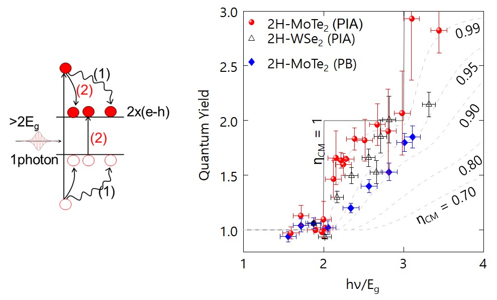
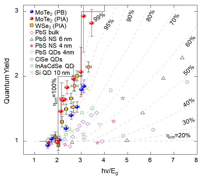
2D materials boost carrier multiplication- IBS researchers discover a carrier multiplication process in 2D semiconductors that could increase the efficiency of future solar cells - Physicists at the Center for Integrated Nanostructure Physics (CINAP), within the Institute for Basic Science (IBS, South Korea), have discovered an intriguing phenomenon, known as carrier multiplication (CM), in a class of semiconductors with incredible thinness, outstanding properties, and possible applications in electronics and optics. Published in Nature Communications, these new findings have the potential to boost the photovoltaics and photodetector fields, and could improve the efficiency of solar cells produced with these ultrathin materials to up to 46%. An interesting class of 2D materials, the van der Waals layered transition metal dichalcogenides (2D-TMDs), are expected to create the next-generation of optoelectronic devices, such as solar cells, transistors, light emitting diodes (LED), etc. They consist of individual thin layers separated by very weak chemical bonds (van der Waals bonds), and have unique optical properties, high light absorption, and high carrier (electron and hole) mobility. Beyond allowing the option to tune their band gap by changing composition and layer thickness, these materials also offer an ultrahigh internal radiative efficiency of >99%, promoted by the elimination of surface imperfections and large binding energy between carriers. Absorption of sunlight in semiconducting 2D-TMD monolayers reaches typically 5-10%, which is an order of magnitude larger than that in most common photovoltaic materials, like silicon, cadmium telluride, and gallium arsenide. Despite these ideal characteristics, however, the maximum power conversion efficiency of 2D-TMDs solar cells has remained below 5% due to losses at the metal electrodes. The IBS team in collaboration with researchers at the University of Amsterdam aimed to overcome this drawback by exploring the CM process in these materials.
CM is a very efficient way to convert light into electricity. A single photon usually excites a single electron, leaving behind an ‘empty space’ (hole). However, it is possible to generate two or more electron-hole pairs in particular semiconductors if the energy of the incident light is sufficiently large, more specifically, if the photon energy is twice the material’s bandgap energy. While the CM phenomenon is rather inefficient in bulk semiconductors, it was expected to be very efficient in 2D materials, but was not proved experimentally due to some technical limitations, like proper 2D-TMD synthesis and ultrafast optical measurement. In this study, the team observed CM in 2D-TMDs, namely 2H-MoTe2 and 2H-WSe2 films, for the first time; a finding that is expected to improve the current efficiency of 2D-TMD solar cells, even going beyond the Shockley-Queisser limit of 33.7%. “Our new results contribute to the fundamental understanding of the CM phenomenon in 2D-TMD. If one overcomes the contact losses and succeeds in developing photovoltaics with CM, their maximum power conversion efficiency could be increased up to 46%,” says Young Hee Lee, CINAP director. “This new nanomaterial engineering offers the possibility for a new generation of efficient, durable, and flexible solar cells.”
Notes for editors - References - Media Contact - About the Institute for Basic Science (IBS) |
|||
|
|
|||
| Next | |
|---|---|
| before |
- Content Manager
- Communications Team : Kwon Ye Seul 042-878-8237
- Last Update 2023-11-28 14:20
55, Expo-ro, Yuseong-gu, Daejeon, Korea, 34126
Tel. +82-42-878-8114 | Fax. +82-42-878-8079 | E-mail. webmaster@ibs.re.kr
Copyright(c) IBS. All Rights Reserved.
