


주메뉴
- About IBS 연구원소개
-
Research Centers
연구단소개
- Research Outcomes
- Mathematics
- Physics
- Center for Underground Physics
- Center for Theoretical Physics of the Universe (Particle Theory and Cosmology Group)
- Center for Theoretical Physics of the Universe (Cosmology, Gravity and Astroparticle Physics Group)
- Dark Matter Axion Group
- Center for Artificial Low Dimensional Electronic Systems
- Center for Theoretical Physics of Complex Systems
- Center for Quantum Nanoscience
- Center for Exotic Nuclear Studies
- Center for Van der Waals Quantum Solids
- Center for Relativistic Laser Science
- Chemistry
- Life Sciences
- Earth Science
- Interdisciplinary
- Center for Neuroscience Imaging Research (Neuro Technology Group)
- Center for Neuroscience Imaging Research (Cognitive and Computational Neuroscience Group)
- Center for Algorithmic and Robotized Synthesis
- Center for Genome Engineering
- Center for Nanomedicine
- Center for Biomolecular and Cellular Structure
- Center for 2D Quantum Heterostructures
- Center for Quantum Conversion Research
- Institutes
- Korea Virus Research Institute
- News Center 뉴스 센터
- Career 인재초빙
- Living in Korea IBS School-UST
- IBS School 윤리경영

주메뉴
- About IBS
-
Research Centers
- Research Outcomes
- Mathematics
- Physics
- Center for Underground Physics
- Center for Theoretical Physics of the Universe (Particle Theory and Cosmology Group)
- Center for Theoretical Physics of the Universe (Cosmology, Gravity and Astroparticle Physics Group)
- Dark Matter Axion Group
- Center for Artificial Low Dimensional Electronic Systems
- Center for Theoretical Physics of Complex Systems
- Center for Quantum Nanoscience
- Center for Exotic Nuclear Studies
- Center for Van der Waals Quantum Solids
- Center for Relativistic Laser Science
- Chemistry
- Life Sciences
- Earth Science
- Interdisciplinary
- Center for Neuroscience Imaging Research (Neuro Technology Group)
- Center for Neuroscience Imaging Research (Cognitive and Computational Neuroscience Group)
- Center for Algorithmic and Robotized Synthesis
- Center for Genome Engineering
- Center for Nanomedicine
- Center for Biomolecular and Cellular Structure
- Center for 2D Quantum Heterostructures
- Center for Quantum Conversion Research
- Institutes
- Korea Virus Research Institute
- News Center
- Career
- Living in Korea
- IBS School


News Center

| Title | How to enlarge 2D materials as single crystals? | ||
|---|---|---|---|
| Embargo date | 2019-05-23 02:00 | Hits | 2475 |
| Press release | |||
| att. | |||
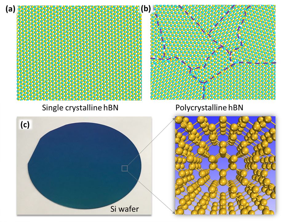
How to enlarge 2D materials as single crystals?Turn it around and find the right symmetric code What makes something a crystal? A transparent and glittery gemstone? Not necessarily in the microscopic world. When all of its atoms are arranged in accordance with specific mathematical rules, we call the material a single crystal. Like the natural world has its unique symmetry just as snowflakes or honeycombs, the atomic world of crystals is designed by its own structure and symmetry. This material structure has a profound effect on its physical properties as well. Specifically, single crystals play an important role in inducing material's intrinsic properties to its full extent. Faced with the coming end of the miniaturization process that the silicon-based integrated circuit has allowed up to this point, huge efforts have been dedicated to find a single crystalline replacement for silicon. In search for the transistor of the future, two-dimensional (2D) materials, especially graphene have been the subject of intense research around the world. Being thin and flexible as a result of being only a single layer of atoms, this 2D version of carbon even features unprecedented electricity and heat conductivity. However, the last decade’s efforts for graphene transistors have been held up by physical restraints graphene allows no control over electricity flow due to the lack of band gap. Then, what about other 2D materials? A number of interesting 2D materials have been reported to have similar or even superior properties. Still, the lack of understanding in creating ideal experimental conditions for large-area 2D materials has limited their maximum size to just a few mm2.
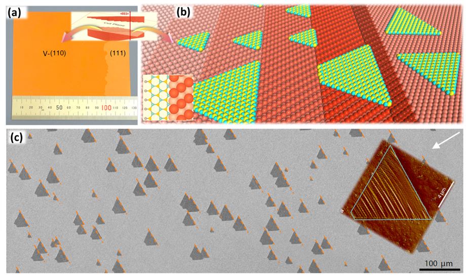
Scientists at the Center for Multidimensional Carbon Materials (CMCM) within the Institute for Basic Science (IBS) (located in the Ulsan National Institute of Science and Technology (UNIST)) have presented a novel approach to synthesize large-scale of silicon wafer size, single crystalline 2D materials. Prof. Feng Ding and Ms. Leining Zhang in collaboration with their colleagues in Peking University, China and other institutes have found a substrate with a lower order of symmetry than that of a 2D material that facilitates the synthesis of single crystalline 2D materials in a large area. "It was critical to find the right balance of rotational symmetries between a substrate and a 2D material," notes Prof. Feng Ding, one of corresponding authors of this study. The researchers successfully synthesized hBN single crystals of 10*10 cm2 by using a new substrate: a surface nearby Cu (110) that has a lower symmetry of (1) than hBN with (3).
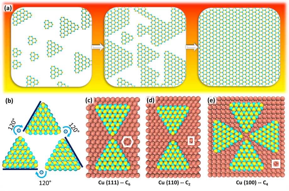
Then, why does symmetry matters? Symmetry, in particular rotational symmetry, describes how many times a certain shape fits on to itself during a full rotation of 360 degrees. The most efficient method to synthesize large-area and single crystals of 2D materials is to arrange layers over layers of small single crystals and grow them upon a substrate. In this epitaxial growth, it is quite challenging to ensure all of the single crystals are aligned in a single direction. Orientation of the crystals is often affected by the underlying substrate. By theoretical analysis, the IBS scientists found that an hBN island (or a group of hBN atoms forming a single triangle shape) has two equivalent alignments on the Cu(111) surface that has a very high symmetry of (6). "It was a common view that a substrate with high symmetry may lead to the growth of materials with a high symmetry. It seemed to make sense intuitively, but this study found it is incorrect," says Ms. Leining Zhang, the first author of the study.
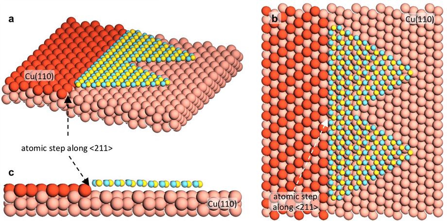
Previously, various substrates such as Cu(111) have been used to synthesize single crystalline hBN in a large area, but none of them were successful. Every effort ended with hBN islands aligning along in several different directions on the surfaces. Convinced by the fact that the key to achieve unidirectional alignment is to reduce the symmetry of the substrate, the researchers made tremendous efforts to obtain vicinal surfaces of a Cu(110) orientation; a surface obtained by cutting a Cu(110) with a small tilt angle. It is like forming physical steps on Cu. As a hBN island tends to place in parallel to the edge of each step, it gets only one preferred alignment. The small tilt angle lowers the symmetry of the surface as well.
They eventually found that a class of vicinal surfaces of Cu (110) can be used to support the growth of hBN with perfect alignment. On a carefully selected substrate with the lowest symmetry or the surface will repeat itself only after a 360degree rotation, hBN has only one preferred direction of alignment. The research team of Prof. Kaihui Liu in Peking University, has developed a unique method to anneal a large Cu foil, up to 10*10 cm2, into a single crystal with the vicinal Cu (110) surface and, with it, they have achieved the synthesis of hBN single crystals of same size. Besides flexibility and ultrathin thickness, emerging 2D materials can present extraordinary properties when they get enlarged as single crystals. "This study provides a general guideline for the experimental synthesis of various 2D materials. Besides the hBN, many other 2D materials could be synthesized with the large area single crystalline substrates with low symmetry," says Prof. Feng Ding. Notably, hBN is the most representative 2D insulator, which is different from the conductive 2D materials, such as graphene, and 2D semiconductors, such as molybdenum disulfide (MoS2). The vertical stacking of various types of 2D materials, such as hBN, graphene and MoS2, would lead to a large number of new materials with exceptional properties and can be used for numerous applications, such as high-performance electronics, sensors, or wearable electronics." Dahee Carol Kim Notes for editors - References - Media Contact - About the Institute for Basic Science (IBS) |
|||
|
|
|||
| Next | |
|---|---|
| before |
- Content Manager
- Communications Team : Kwon Ye Seul 042-878-8237
- Last Update 2023-11-28 14:20
55, Expo-ro, Yuseong-gu, Daejeon, Korea, 34126
Tel. +82-42-878-8114 | Fax. +82-42-878-8079 | E-mail. webmaster@ibs.re.kr
Copyright(c) IBS. All Rights Reserved.
