


주메뉴
- About IBS 연구원소개
-
Research Centers
연구단소개
- Research Outcomes
- Mathematics
- Physics
- Center for Theoretical Physics of the Universe(Particle Theory and Cosmology Group)
- Center for Theoretical Physics of the Universe(Cosmology, Gravity and Astroparticle Physics Group)
- Center for Exotic Nuclear Studies
- Center for Artificial Low Dimensional Electronic Systems
- Center for Underground Physics
- Center for Axion and Precision Physics Research
- Center for Theoretical Physics of Complex Systems
- Center for Quantum Nanoscience
- Center for Van der Waals Quantum Solids
- Chemistry
- Life Sciences
- Earth Science
- Interdisciplinary
- Institutes
- Korea Virus Research Institute
- News Center 뉴스 센터
- Career 인재초빙
- Living in Korea IBS School-UST
- IBS School 윤리경영

주메뉴
- About IBS
-
Research Centers
- Research Outcomes
- Mathematics
- Physics
- Center for Theoretical Physics of the Universe(Particle Theory and Cosmology Group)
- Center for Theoretical Physics of the Universe(Cosmology, Gravity and Astroparticle Physics Group)
- Center for Exotic Nuclear Studies
- Center for Artificial Low Dimensional Electronic Systems
- Center for Underground Physics
- Center for Axion and Precision Physics Research
- Center for Theoretical Physics of Complex Systems
- Center for Quantum Nanoscience
- Center for Van der Waals Quantum Solids
- Chemistry
- Life Sciences
- Earth Science
- Interdisciplinary
- Institutes
- Korea Virus Research Institute
- News Center
- Career
- Living in Korea
- IBS School


News Center

|
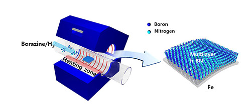
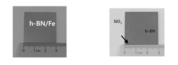
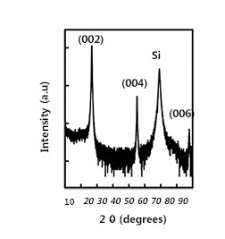
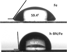
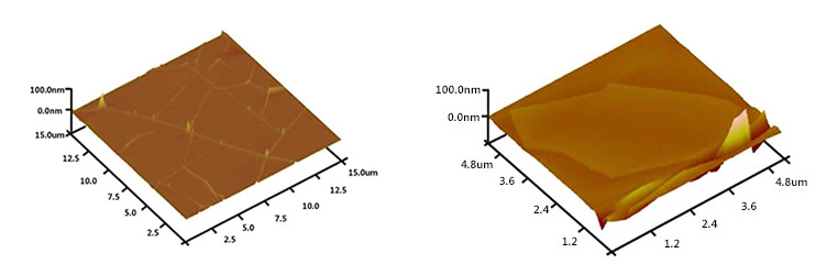
IBS Scientists Synthesize Hexagonal Boron Nitride Seeking a New Pathway: the interactions of insulators and conductors October 28, 2015 Conductors and insulators exist everywhere in life and allow for the performance of both trivial and vital tasks: the stirring of a pot of soup or the flow of electricity, like the current of a river, powering generators in hospitals and even the computer screen you’re looking at right now. A conducting material, like metal, allows electrons to flow freely from material to material permitting the charge to travel across the entirety of its surface. If the material touches another conducting material the charge transfers and repeats the exercise perpetually. That is, of course, unless it interacts with an insulator. Interactions of insulators and conductors Imagine the relationship between our two actors as a car cruising down a long straight highway with traffic lights dotted throughout. The car - portraying the conductor - races along freely until it comes to a red light- the insulator- and the circuit breaks down. Insulators are materials which impede the free flowing movement of electrons from atom to atom and molecule to molecule. If a charge flowing through a conductor is suddenly transferred to an insulator, the excess charge will remain at the initial location. Insulators do not permit electrons to flow freely, similar to the car forced to sit patiently at a red light. Researchers from the Center for Integrated Nanostructure Physics (CINAP) within the Institute for Basic Science have assiduously studied the relationship between insulators and conductors. The international team, headed by the director of CINAP, Young Hee Lee, has extensively tested layered hexagonal boron nitride (h-BN) – an insulating two-dimensional material (2-D) of remarkable properties. All the atoms in 2-D layer materials are exposed to the surface, the related physical and chemical properties are strongly influenced by adjoining materials and sometimes surface corrugation. Therefore, special care is required to deal with atomically thin layered materials. There are several unique physical and chemical properties of h-BN, which have potential applications as a dry-lubricant, passivation layer and deep ultraviolet emitter. According to the team’s paper, published in Nature Communications, the h-BN layer is also superior to its competing insulator, silicon dioxide (SiO2), as it “has demonstrated to be an ideal substrate {supporting material} for 2-D materials due to its atomic flatness, large band gap, superb mechanical strength, absence of dangling bonds and low dielectric screening.” The compound is highly desired for numerous real device applications in keyboards and power cabling manufacturing. Process of synthesis In the paper, the team reports large-area h-BN films grown by chemical vapor deposition (CVD) using copper foil (Fe foil). CVD is a method employed to produce high quality, high performance solid materials. The thickness of the h-BN (5-15 nm) is controlled by the cooling rate, i.e., the segregated boron and nitrogen atoms that are precipitated in an iron substrate at a high temperature. Field effect transistors (FETs) with CVD-grown monolayer graphene, monolayer molybdenum disulfide (MoS2), and monolayer tungsten diselenide (WSe2) – both semiconducting materials- are fabricated on the grown multi-layer h-BN substrates, achieving carrier mobilities as high as ~ 24,000, 40, and ~ 9 cm2 V-1s-1 at room temperature, respectively. The reported graphene mobility is the highest value among those of the previous reports with CVD-grown graphene samples on CVD-grown h-BN substrates. Real life application of h-BN in 2-D materials Hexagonal boron nitride is an ideal substrate for 2-D materials including graphene and transition metal dichalcogenides monolayers family (TMdC). While exfoliated h-BN resulted in a very high performance, integration is not possible with a limited area. Large-area CVD-grown h-BN can be easily integrated with various 2-D materials. To demonstrate h-BN film as a potential substrate, graphene, MoS2, and WSe2 devices were fabricated on-top of our large-area CVD-grown h-BN. The large-area and high-quality h-BN substrate in this work not only advances the high performance of 2-D nanoelectronics for the future, but also provides a new synthesis technique for potential multi-layer 2-D materials.
By Neil Mannix Notes for editors - References - Media Contact - About the Institute for Basic Science (IBS)
|
|||
|
|

| Next | |
|---|---|
| before |
- Content Manager
- Public Relations Team : Suh, William Insang 042-878-8137
- Last Update 2023-11-28 14:20
55, Expo-ro, Yuseong-gu, Daejeon, Korea, 34126
Tel. +82-42-878-8114 | Fax. +82-42-878-8079 | E-mail. webmaster@ibs.re.kr
Copyright(c) IBS. All Rights Reserved.
