


주메뉴
- About IBS 연구원소개
-
Research Centers
연구단소개
- Research Outcomes
- Mathematics
- Physics
- Center for Theoretical Physics of the Universe(Particle Theory and Cosmology Group)
- Center for Theoretical Physics of the Universe(Cosmology, Gravity and Astroparticle Physics Group)
- Center for Exotic Nuclear Studies
- Center for Artificial Low Dimensional Electronic Systems
- Center for Underground Physics
- Center for Axion and Precision Physics Research
- Center for Theoretical Physics of Complex Systems
- Center for Quantum Nanoscience
- Center for Van der Waals Quantum Solids
- Chemistry
- Life Sciences
- Earth Science
- Interdisciplinary
- Institutes
- Korea Virus Research Institute
- News Center 뉴스 센터
- Career 인재초빙
- Living in Korea IBS School-UST
- IBS School 윤리경영

주메뉴
- About IBS
-
Research Centers
- Research Outcomes
- Mathematics
- Physics
- Center for Theoretical Physics of the Universe(Particle Theory and Cosmology Group)
- Center for Theoretical Physics of the Universe(Cosmology, Gravity and Astroparticle Physics Group)
- Center for Exotic Nuclear Studies
- Center for Artificial Low Dimensional Electronic Systems
- Center for Underground Physics
- Center for Axion and Precision Physics Research
- Center for Theoretical Physics of Complex Systems
- Center for Quantum Nanoscience
- Center for Van der Waals Quantum Solids
- Chemistry
- Life Sciences
- Earth Science
- Interdisciplinary
- Institutes
- Korea Virus Research Institute
- News Center
- Career
- Living in Korea
- IBS School


News Center

| Title | IBS Cleave few-layer samples of Magnetic Material NiPS3 | ||
|---|---|---|---|
| Embargo date | 2016-03-17 12:00 | Hits | 3618 |
| Research Center |
Center for Correlated Electron Systems |
||
| Press release | |||
| att. | |||
|
IBS Cleave few-layer samples of Magnetic Material NiPS3 - The IBS Center for Correlated Electron Systems (CCES) reports first successful atomically thin sheets of the magnetic Van der Waals material - March 17, 2016
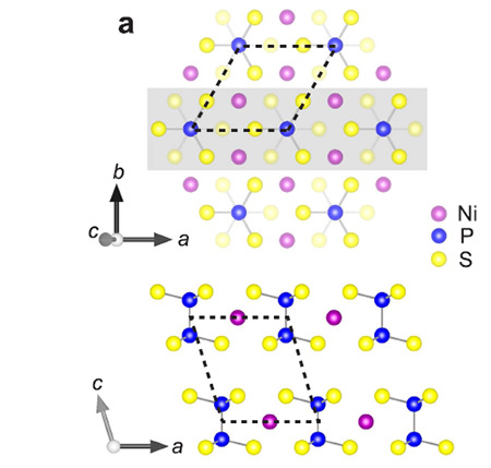
Heterostructures (referred to as Van der Waals {VdW}) are attracting a great deal of attention due to their diverse physical and chemical properties. A VdW heterostructure is assembled by stacking two or more different 2D semiconducting crystals on top of each other. The structure is grown by repeating the practice, the resulting stack represents an artificial material constructed in a certain sequence, akin to Lego blocks. There has been huge interest in these materials as they hold vast potential in helping science to find a new semiconductor that can replace silicon which decomposes and segregates in a natural environment. A VdW heterostructure can overcome the limitations of 2D crystals and offer an alternative for the construction of smaller and more powerful storage devices, supercomputers, administration of medicine and enhanced memory and graphics in hand held devices. Electrons within semiconductors roam freely and have internal states or ‘spins’. These spin currents exhibit magnetic order and can be tuned to prevent energy dissipation which occurs naturally when information is processed at vast speeds. However, not all VdW’s have this spin state; scientifically known as an antiferromagnetic state. PARK Je-Geun, a scientist from CCES, explains the unique qualities of their tested material NiPS3: “The compound nickel phosphorus trisulfide (NiPS3) is an intrinsically magnetic material and is an invaluable building block for the design for multi-layered VdW heterostructures.” The Center is the first to obtain monolayer and multilayer samples of magnetic VdW materials; the results lay the foundation for the development of future semiconductors that are high speed, low energy consuming and highly compact.
World’s first in KoreaThe VdW material the IBS team experimented on belongs to a class of transition metals phosphorus trisulfides (MPS3) and, more importantly, exhibits antiferromagnetic order. With further developments, it can, theoretically, replace silicon as an ideal material for future magnetic semiconductors. The results compiled by the IBS team have never before been reported in the form of ultrathin sheets. The team’s scientific paper, published on February 15 in Scientific Reports, outlined the potential of their work as such: “Beyond their already fascinating properties, these VdW heterostructures and superlattices may exhibit even more exotic behavior. In particular, for the design of spintronic devices, VdW materials that exhibit magnetic order would be highly desirable building blocks.”
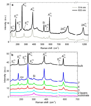
Methods of CCES & A Bright Future for 2D MaterialsUsing the well-established Scotch tape technique, the Korean team exfoliated flakes of NiPS3 onto silicon capped by silicon oxide (SiO2). The resulting material was subjected to a heavy bombardment of high intensity lasers: a process called Raman spectroscopy, designed to provide specific information about molecular vibrations. Other forms of atomic scanning were performed to ascertain how different the atomic make-up of NiPS3 is, in comparison, to its bulk form: MPS3. The team recorded stark differences in the Raman spectra of thin NiPS3 from the bulk material and the Raman spectra varied clearly between sheets of different layer numbers. According to the paper these results exhibit a “key significance of our results is that bulk MPS3 compounds exhibit magnetism, and antiferromagnetic ordering strongly influenced by interlayer coupling is known to take place at moderately low temperature.” Up until now, it is quite expensive to obtain magnetic monolayer oxides materials as it requires a high-end device and the material itself is less likely to be commercially available for technical use. This study proves that monolayer magnetic material can be obtained using magnetic atom like nickel (Ni) as well as many other magnetic atoms such as iron (Fe). The work of the IBS team is, tentatively, laying the foundations for the future study of spin-memory materials. Research is continuously driven by our collective scientific curiosity; we are within reach of precise control of electrons and atoms which would herald a new era of scientific exploration. The research team’s next mission is to obtain a magnetic monolayer material at moderate temperature. If they succeed, it will be very crucial step in commercializing magnetic semiconductors. Neil Mannix Notes for editors - References - Media Contact - About the Institute for Basic Science (IBS) |
|||
|
|
|||
| Next | |
|---|---|
| before |
- Content Manager
- Communications Team : Kwon Ye Seul 042-878-8237
- Last Update 2023-11-28 14:20
55, Expo-ro, Yuseong-gu, Daejeon, Korea, 34126
Tel. +82-42-878-8114 | Fax. +82-42-878-8079 | E-mail. webmaster@ibs.re.kr
Copyright(c) IBS. All Rights Reserved.
