


주메뉴
- About IBS 연구원소개
-
Research Centers
연구단소개
- Research Outcomes
- Mathematics
- Physics
- Center for Theoretical Physics of the Universe(Particle Theory and Cosmology Group)
- Center for Theoretical Physics of the Universe(Cosmology, Gravity and Astroparticle Physics Group)
- Center for Exotic Nuclear Studies
- Center for Artificial Low Dimensional Electronic Systems
- Center for Underground Physics
- Center for Axion and Precision Physics Research
- Center for Theoretical Physics of Complex Systems
- Center for Quantum Nanoscience
- Center for Van der Waals Quantum Solids
- Chemistry
- Life Sciences
- Earth Science
- Interdisciplinary
- Institutes
- Korea Virus Research Institute
- News Center 뉴스 센터
- Career 인재초빙
- Living in Korea IBS School-UST
- IBS School 윤리경영

주메뉴
- About IBS
-
Research Centers
- Research Outcomes
- Mathematics
- Physics
- Center for Theoretical Physics of the Universe(Particle Theory and Cosmology Group)
- Center for Theoretical Physics of the Universe(Cosmology, Gravity and Astroparticle Physics Group)
- Center for Exotic Nuclear Studies
- Center for Artificial Low Dimensional Electronic Systems
- Center for Underground Physics
- Center for Axion and Precision Physics Research
- Center for Theoretical Physics of Complex Systems
- Center for Quantum Nanoscience
- Center for Van der Waals Quantum Solids
- Chemistry
- Life Sciences
- Earth Science
- Interdisciplinary
- Institutes
- Korea Virus Research Institute
- News Center
- Career
- Living in Korea
- IBS School


News Center

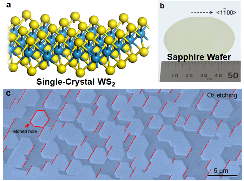
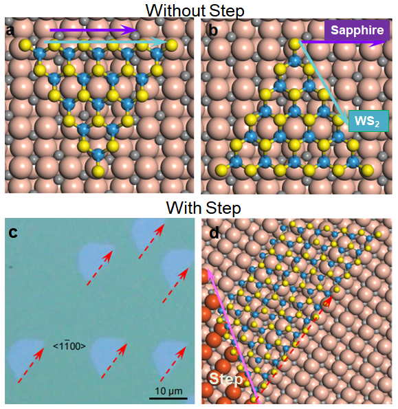
Ultra-Large Single-crystal WS2 Monolayer-New technique opens a possibility to replace silicon with 2D materials in semiconducting technology- As silicon based semiconducting technology is approaching the limit of its performance, new materials that may replace or partially replace silicon in technology is highly desired. Recently, the emergence of graphene and other two-dimensional (2D) materials offers a new platform for building next generation semiconducting technology. Among them, transition metal dichalcogenides (TMDs), such as MoS2, WS2, MoSe2, WSe2, as most appealing 2D semiconductors. A prerequisite of building ultra-large-scale high-performance semiconducting circuits is that the base materials must be a single-crystal of wafer-scale, just like the silicon wafer used today. Although great efforts have been dedicated to the growth of wafer-scale single-crystals of TMDs, the success was very limited until now. Distinguished Professor Feng Ding and his research team from the Center for Multidimensional CarbonMaterials (CMCM), within the Institute for Basic Science (IBS) at UNIST, in cooperation with researcher at Peking University (PKU), Beijing Institute of Technology, and Fudan University, reported the direct growth of 2-inch single-crystal WS2 monolayer films very recently. Besides the WS2, the research team also demonstrated the growth of single-crystal MoS2, WSe2, and MoSe2 in wafer scale as well. The key technology of epitaxially grown a large sing-crystal is to ensure that all small single-crystal grown on a substrate are uniformly aligned. Because TMDs has non-centrosymmetric structure or the mirror image of a TMD with respect to an edge of it has opposite alignment, we must break such a symmetry by carefully design the substrate. Based on theoretical calculations, the authors proposed a mechanisms of “dual-coupling-guided epitaxy growth” for experimental design. The WS2-sapphire plane interaction as the first driving force, leading to two preferred antiparallel orientations of the WS2 islands. The coupling between WS2 and sapphire step-edge is the second driving force and it will break the degeneracy of the two antiparallel orientations. Then all the TMD single crystals grown on a substrate with step edges are all unidirectional aligned and finally, the coalescence of these small single-crystals leads to a large single-crystal of the same size of the substrate. “This new dual-coupling epitaxy growth mechanism is new for controllable materials growth. In principle, it allows us realize to grow all 2D materials into large-area single crystals if proper substrate was found.” Says Dr. Ting Cheng, the co-first author of the study. “We have considered how to choose proper substrates theoretically. First, the substrate should have a low symmetry and, secondly, more step edges are preferred.” emphasizes Professor Feng Ding, the corresponding author of the study. “This is a major step forward in the area of 2D materials based device. As the successful growth of wafer-scale single-crystal 2D TMDs on insulators beyond graphene and hBN on transition metal substrates, our study provide the required keystone of 2D semiconductors in high-end applications of electronic and optical devices,” explains professor Feng Ding.
Notes for editors - References - Media Contact - About the Institute for Basic Science (IBS) |
|||
|
|
| Next | |
|---|---|
| before |
- Content Manager
- Public Relations Team : Suh, William Insang 042-878-8137
- Last Update 2023-11-28 14:20
55, Expo-ro, Yuseong-gu, Daejeon, Korea, 34126
Tel. +82-42-878-8114 | Fax. +82-42-878-8079 | E-mail. webmaster@ibs.re.kr
Copyright(c) IBS. All Rights Reserved.
