


주메뉴
- About IBS 연구원소개
-
Research Centers
연구단소개
- Research Outcomes
- Mathematics
- Physics
- Center for Theoretical Physics of the Universe(Particle Theory and Cosmology Group)
- Center for Theoretical Physics of the Universe(Cosmology, Gravity and Astroparticle Physics Group)
- Center for Exotic Nuclear Studies
- Center for Artificial Low Dimensional Electronic Systems
- Center for Underground Physics
- Center for Axion and Precision Physics Research
- Center for Theoretical Physics of Complex Systems
- Center for Quantum Nanoscience
- Center for Van der Waals Quantum Solids
- Chemistry
- Life Sciences
- Earth Science
- Interdisciplinary
- Institutes
- Korea Virus Research Institute
- News Center 뉴스 센터
- Career 인재초빙
- Living in Korea IBS School-UST
- IBS School 윤리경영

주메뉴
- About IBS
-
Research Centers
- Research Outcomes
- Mathematics
- Physics
- Center for Theoretical Physics of the Universe(Particle Theory and Cosmology Group)
- Center for Theoretical Physics of the Universe(Cosmology, Gravity and Astroparticle Physics Group)
- Center for Exotic Nuclear Studies
- Center for Artificial Low Dimensional Electronic Systems
- Center for Underground Physics
- Center for Axion and Precision Physics Research
- Center for Theoretical Physics of Complex Systems
- Center for Quantum Nanoscience
- Center for Van der Waals Quantum Solids
- Chemistry
- Life Sciences
- Earth Science
- Interdisciplinary
- Institutes
- Korea Virus Research Institute
- News Center
- Career
- Living in Korea
- IBS School


News Center

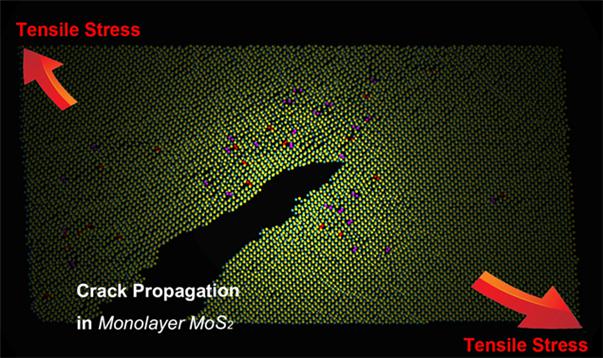
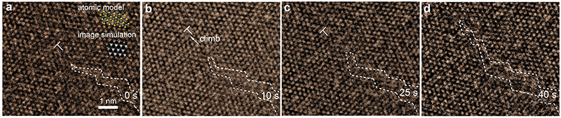
Explaining How 2D Materials Break at the Atomic Level- IBS physicists found that to shed light on the cracking of MoS2, we must go beyond the theory used so far - Cracks sank the 'unsinkable' Titanic; decrease the performance of touchscreens and erode teeth. We are familiar with cracks in big or small three-dimensional (3D) objects, but how do thin two-dimensional (2D) materials crack? 2D materials, like molybdenum disulfide (MoS2), have emerged as an important asset for future electronic and photoelectric devices. However, the mechanical properties of 2D materials are expected to differ greatly from 3D materials. Scientists at the Center for Integrated Nanostructure Physics (CINAP), within the Institute for Basic Science (IBS) published, on Nature Communications, the first observation of 2D MoS2 cracking at the atomic level. This study is expected to contribute to the applications of new 2D materials. Obviously when a certain force is applied to a material a crack is created. Less obvious is how to explain and predict the shape and seriousness of a crack from a physics point of view. Scientists want to investigate which fractures are likely to expand and which are not .Materials are divided into ductile and brittle: Ductile materials, like gold, withstand large strains before rupturing; brittle materials, like glass, can absorb relatively little energy before breaking suddenly, without elongation and deformation. At the nano-level atoms move freer in ductile materials than in brittle materials; so in the presence of a pulling force (tensile stress) they can go out of position from the ordered crystal structure, or in technical terms - they dislocate. So far, this explanation (Griffith model) has been applied to cracking phenomena in bulk, but it lacks experimental data at the atomic or nano-scale. In this study, IBS scientists observed how cracks propagate on 2D MoS2 after a pore was formed either spontaneously or with an electron beam. "The most difficult point {of the experiments} was to use the electron beam to create the pore without generating other defects or breaking the sample," explains Thuc Hue Ly, first author of this study. "So we had to be fast and use a minimum amount of energy." The atomic observations were done using real-time transmission electron microscopy. Surprisingly, even though MoS2 is a brittle material, the team saw atom dislocations 3-5 nanometers (nm) away from the front line of the crack, or crack tip. This observation cannot be explained with the Griffith model.
In order to create conditions that represent the natural environment, the sample was exposed to ultraviolet (UV) light. This caused the MoS2 to oxidize; atom dislocations occurred more rapidly and the stretched region expanded to 5-10 nm from the crack tip.
"The study shows that cracking in 2D materials is fundamentally different from cracking in 3D ductile and brittle materials. These results cannot be explained with the conventional material failure theory, and we suggest that a new theory is needed," explained CINAP Professor LEE Young Hee. Letizia Diamante Notes for editors - References - Media Contact - About the Institute for Basic Science (IBS) |
|||
Center for Integrated Nanostructure PhysicsPublication Repository |
|||
|
|

| Next | |
|---|---|
| before |
- Content Manager
- Public Relations Team : Suh, William Insang 042-878-8137
- Last Update 2023-11-28 14:20
55, Expo-ro, Yuseong-gu, Daejeon, Korea, 34126
Tel. +82-42-878-8114 | Fax. +82-42-878-8079 | E-mail. webmaster@ibs.re.kr
Copyright(c) IBS. All Rights Reserved.
