


주메뉴
- About IBS 연구원소개
-
Research Centers
연구단소개
- Research Outcomes
- Mathematics
- Physics
- Center for Theoretical Physics of the Universe(Particle Theory and Cosmology Group)
- Center for Theoretical Physics of the Universe(Cosmology, Gravity and Astroparticle Physics Group)
- Center for Exotic Nuclear Studies
- Center for Artificial Low Dimensional Electronic Systems
- Center for Underground Physics
- Center for Axion and Precision Physics Research
- Center for Theoretical Physics of Complex Systems
- Center for Quantum Nanoscience
- Center for Van der Waals Quantum Solids
- Chemistry
- Life Sciences
- Earth Science
- Interdisciplinary
- Institutes
- Korea Virus Research Institute
- News Center 뉴스 센터
- Career 인재초빙
- Living in Korea IBS School-UST
- IBS School 윤리경영

주메뉴
- About IBS
-
Research Centers
- Research Outcomes
- Mathematics
- Physics
- Center for Theoretical Physics of the Universe(Particle Theory and Cosmology Group)
- Center for Theoretical Physics of the Universe(Cosmology, Gravity and Astroparticle Physics Group)
- Center for Exotic Nuclear Studies
- Center for Artificial Low Dimensional Electronic Systems
- Center for Underground Physics
- Center for Axion and Precision Physics Research
- Center for Theoretical Physics of Complex Systems
- Center for Quantum Nanoscience
- Center for Van der Waals Quantum Solids
- Chemistry
- Life Sciences
- Earth Science
- Interdisciplinary
- Institutes
- Korea Virus Research Institute
- News Center
- Career
- Living in Korea
- IBS School


News Center

|
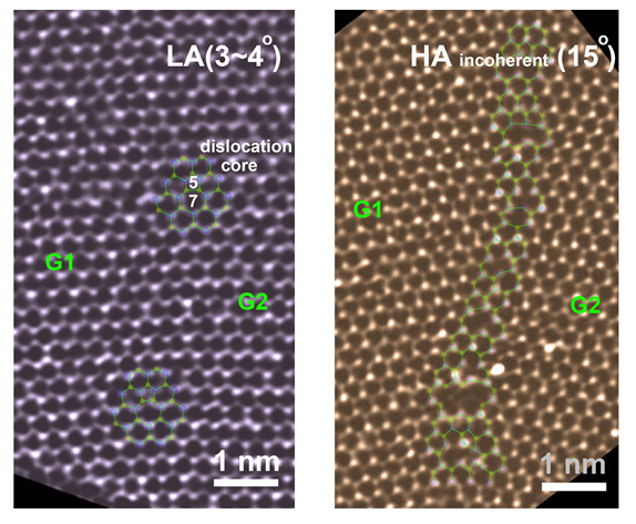
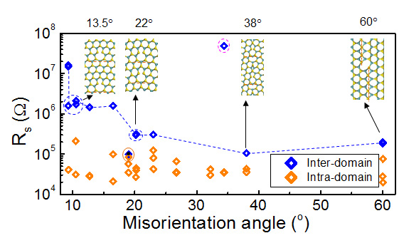
IBS Report Electric Transport across Molybdenum Disulfide Grain Boundaries - Scientific team from CINAP/IBS identifies previously undiscovered differences in grain boundaries - Jan 27, 2016 The Center for Integrated Nanostructure Physics (CINAP) within IBS has reported results correlating the flake merging angle with grain boundary (GBs) properties, and proven that increasing the merging angle of GBs drastically improves the flow of electrons. This correlates to an increase in the carrier mobility from less than 1 cm2V-1s-1 for small angles, to 16cm2 V-1s-1 for angles greater than 20°. The paper, entitled, ‘Misorientation-angle-dependent electrical transport across molybdenum disulfide grain boundaries’ is published in the journal Nature Communication. According to the paper, it is essential to understand the atomic structures of GBs in order to control and improve electrical transport properties in both bulk and low-dimensional materials. Grain boundaries are the direction that atoms are arranged in a material. For the experiments undertaken by scientists at CINAP, a monolayer molybdenum disulfide (MoS2) was grown by chemical vapour deposition (CVD) and subsequently transferred to a substrate of silicon dioxide (SiO2). The team’s reasoning for using MoS2 is twofold: firstly, it is a 2D semiconductor that features high electrical conductance and, crucially, has a natural bandgap, which enables it to be tuned on and off and; secondly, the grain boundaries are well-defined. This is paramount for successful experiments. Previous research from Northwestern University found that the GBs of MoS2 provided a unique way to modulate resistance; this was achieved by using a large electric field to spatially modulate the location of the grain boundaries. The Northwestern results, published last year in Nature Nanotechnology, opened a pathway for future research, but the debate regarding the transport physics at the GB is still under dispute. This is due to a large device-to-device performance variation, poor single-domain carrier mobility, and, most importantly, a lack of correlation between transport properties and GB atomic structures in MoS2 research. The CINAP team, headed by the Center’s director Young Hee Lee, overcame these obstacles by directly correlating four-probe transport measurements across single GBs with both high-resolution transmission electron microscopy (TEM) imaging and first-principles calculations. TEM is a microscopy technique whereby a beam of electrons is transmitted through an ultra-thin specimen, interacting with the specimen as it passes through. An exact atomic-scale image is formed from the interaction of the electrons transmitted through the specimen. Identifying Grain BoundariesGBs in the MoS2 layers were identified and regions with no sign of wrinkling or multilayers were then selected to prevent misinterpretations. Four-probe transport measurements were then performed on the substrate with surprising results; when measuring flake misorientations of 8–20o, mobility increased from much less than 1 cm2V-1s-1 up to 16cm2 V-1s-1. Above 20o field effect mobility saturates at a 16cm2 V-1s-1 intra-domain cutoff. Thus, GBs between flakes having a misorientation angle of 20–60o show better transport properties. The team has, as reported in their paper, “provided a more unified picture of the relationship between mobility, merging angle and atomistic structures of the GBs of monolayer MoS2.” The results provide practical expectations regarding transport properties in large-area films, which will be restricted largely by the poor mobility across GBs. The results obtained in this work are applicable to other similar 2D systems, and contribute to the fundamental understanding of transport in semiconductors.
Notes for editors - References - Media Contact - About the Institute for Basic Science (IBS) |
|||
Center for Integrated Nanostructure PhysicsPublication Repository |
|||
|
|

| Next | |
|---|---|
| before |
- Content Manager
- Public Relations Team : Suh, William Insang 042-878-8137
- Last Update 2023-11-28 14:20

55, Expo-ro, Yuseong-gu, Daejeon, Korea, 34126
Tel. +82-42-878-8114 | Fax. +82-42-878-8079 | E-mail. webmaster@ibs.re.kr
Copyright(c) IBS. All Rights Reserved.
