


주메뉴
- About IBS 연구원소개
-
Research Centers
연구단소개
- Research Outcomes
- Mathematics
- Physics
- Center for Theoretical Physics of the Universe(Particle Theory and Cosmology Group)
- Center for Theoretical Physics of the Universe(Cosmology, Gravity and Astroparticle Physics Group)
- Center for Exotic Nuclear Studies
- Center for Artificial Low Dimensional Electronic Systems
- Center for Underground Physics
- Center for Axion and Precision Physics Research
- Center for Theoretical Physics of Complex Systems
- Center for Quantum Nanoscience
- Center for Van der Waals Quantum Solids
- Chemistry
- Life Sciences
- Earth Science
- Interdisciplinary
- Institutes
- Korea Virus Research Institute
- News Center 뉴스 센터
- Career 인재초빙
- Living in Korea IBS School-UST
- IBS School 윤리경영

주메뉴
- About IBS
-
Research Centers
- Research Outcomes
- Mathematics
- Physics
- Center for Theoretical Physics of the Universe(Particle Theory and Cosmology Group)
- Center for Theoretical Physics of the Universe(Cosmology, Gravity and Astroparticle Physics Group)
- Center for Exotic Nuclear Studies
- Center for Artificial Low Dimensional Electronic Systems
- Center for Underground Physics
- Center for Axion and Precision Physics Research
- Center for Theoretical Physics of Complex Systems
- Center for Quantum Nanoscience
- Center for Van der Waals Quantum Solids
- Chemistry
- Life Sciences
- Earth Science
- Interdisciplinary
- Institutes
- Korea Virus Research Institute
- News Center
- Career
- Living in Korea
- IBS School


News Center

| Title | Improved 3D Nanoprinting Technique to Build Nanoskyscrapers | ||
|---|---|---|---|
| Embargo date | 2019-12-19 15:08 | Hits | 678 |
| Research Center |
Center for Soft and Living Matter |
||
| Press release | |||
| att. | |||
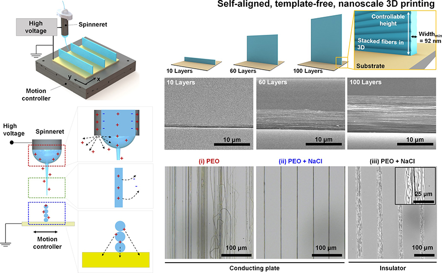
Improved 3D Nanoprinting Technique to Build Nanoskyscrapers- Simply adding “table salt” helps to build self-stacked nanoarchitectures - Nanowalls, nanobridges, nano “jungle gyms”: it could seem the description of a Lilliputian village, but these are actual 3D-printed components with tremendous potential applications in nanoelectronics, smart materials and biomedical devices. Researchers at the Center for Soft and Living Matter (CSLM), within the Institute for Basic Science (IBS, South Korea) have improved the 3D nanoprinting process that enables to build precise, self-stacked, tall-and-narrow nanostructures. As shown in their latest publication in Nano Letters, the team also used this technique to produce transparent nanoelectrodes with high optical transmission and controllable conductivity. The near-field electrospinning (NFES) technique consists of a syringe filled with a polymer solution suspended above a platform, which collects the ejected nanofiber and is pre-programmed to move left-and-right, back-and-forth, depending on the shape of the desired final product. The syringe and the platform have opposite charges, so that the polymer jet coming out from the needle of the syringe is attracted to the platform, forming a continuous fiber that solidifies on the platform. Since the electrospun jets are difficult to handle, this technique was limited to two-dimensional (2D) structures or hollow cylindrical three-dimensional (3D) structures, often with relatively large fiber diameters of a few micrometers. IBS researchers were able to achieve a better control of the nanofiber deposition on the platform, by adding an appropriate concentration of sodium chloride (NaCl) to the polymer solution. This ensured the spontaneous alignment of the nanofiber layers stacked on top of each other forming walls. “Although it is highly applicable to various fields, it is difficult to build stacked nanofibers with multiple designs using the conventional electrospinning techniques,” says Yoon-Kyoung Cho, the corresponding author of the study. "Our experiment showed that salt did the trick.” The benefit provided by salt is related to the charges. The difference in voltage between the syringe and the platform creates positive charges in the polymer solution and negative charges in the platform, but a residual positive charge stays in the solidified fibers on the platform. The team found that applying salt to the polymer solution enhances the charge dissipation, leading to higher electrostatic attraction between the nanofiber jet and the fibers deposited on the platform.
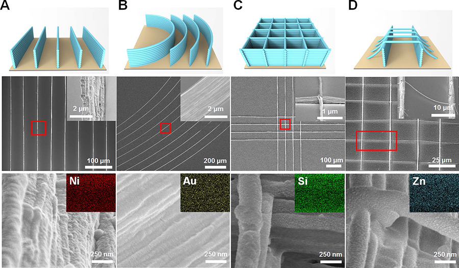
Based on this mechanism, the team was able to produce tall-and-narrow nanowalls, with a minimum width of around 92 nanometers and a maximum height of 6.6 micrometers, and construct a variety of 3D nanoarchitectures, such as curved nanowall arrays, nano “jungle gyms,” and nanobridges, with controllable dimensions.
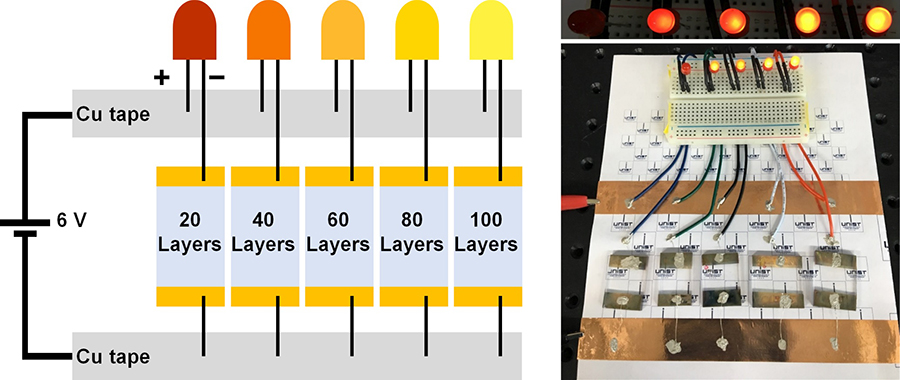
To demonstrate the potential application of these nanostructures, the researchers in collaboration with Hyunhyub Ko, professor at Ulsan National Institute of Science and Technology (UNIST), prepared 3D nanoelectrodes with silver-coated nanowalls embedded in transparent and flexible polydimethylsiloxane (PDMS) films. They confirmed that electrical resistance could be tuned with the number of nanofiber layers (the taller the nanowalls, the smaller the resistance), without affecting light transmission. “Interestingly, this method can potentially avoid the trade-off between optical transmittance and sheet resistance in transparent electrodes. Arrays of 3D silver nanowires made with 20, 40, 60, 80, or 100 layers of nanofibers had variable conductivity, but stable light transmission of around 98%,” concludes Yang-Seok Park, the first author of the study.
The Center for Soft and Living Matter is located at Ulsan National Institute of Science and Technology (UNIST). Letizia Diamante Notes for editors - References - Media Contact - About the Institute for Basic Science (IBS) |
|||
|
|
|||
| Next | |
|---|---|
| before |
- Content Manager
- Communications Team : Kwon Ye Seul 042-878-8237
- Last Update 2023-11-28 14:20
55, Expo-ro, Yuseong-gu, Daejeon, Korea, 34126
Tel. +82-42-878-8114 | Fax. +82-42-878-8079 | E-mail. webmaster@ibs.re.kr
Copyright(c) IBS. All Rights Reserved.
