


주메뉴
- About IBS 연구원소개
-
Research Centers
연구단소개
- Research Outcomes
- Mathematics
- Physics
- Center for Theoretical Physics of the Universe(Particle Theory and Cosmology Group)
- Center for Theoretical Physics of the Universe(Cosmology, Gravity and Astroparticle Physics Group)
- Center for Exotic Nuclear Studies
- Center for Artificial Low Dimensional Electronic Systems
- Center for Underground Physics
- Center for Axion and Precision Physics Research
- Center for Theoretical Physics of Complex Systems
- Center for Quantum Nanoscience
- Center for Van der Waals Quantum Solids
- Chemistry
- Life Sciences
- Earth Science
- Interdisciplinary
- Institutes
- Korea Virus Research Institute
- News Center 뉴스 센터
- Career 인재초빙
- Living in Korea IBS School-UST
- IBS School 윤리경영

주메뉴
- About IBS
-
Research Centers
- Research Outcomes
- Mathematics
- Physics
- Center for Theoretical Physics of the Universe(Particle Theory and Cosmology Group)
- Center for Theoretical Physics of the Universe(Cosmology, Gravity and Astroparticle Physics Group)
- Center for Exotic Nuclear Studies
- Center for Artificial Low Dimensional Electronic Systems
- Center for Underground Physics
- Center for Axion and Precision Physics Research
- Center for Theoretical Physics of Complex Systems
- Center for Quantum Nanoscience
- Center for Van der Waals Quantum Solids
- Chemistry
- Life Sciences
- Earth Science
- Interdisciplinary
- Institutes
- Korea Virus Research Institute
- News Center
- Career
- Living in Korea
- IBS School


News Center

| Title | New 2D Transistor Material Made Using Precision Lasers | ||
|---|---|---|---|
| Embargo date | 2015-08-07 14:26 | Hits | 9955 |
| Press release | |||
| att. | |||
|
New 2D Transistor Material Made Using Precision Lasers - A New Technique for Making 2D Transistor from dual-phase TMD
Crystal -
August 7, 2015
Molybdenum ditelluride (MoTe2) is a crystalline compound that if pure enough can be used as a transistor. Its molecular structure is an atomic sandwich made up of one molybdenum atom for every two tellurium atoms. It was first made in the 1960’s via several different fabrication methods, but until last year it had never been made in a pure enough form to be suitable for electronics.
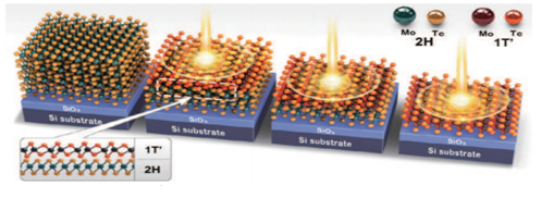
Last year a multi-discipline research team led by South Korea’s Institute for Basic Science (IBS) Center for Integrated Nanostructure Physics at Sungkyunkwan University (SKKU) director Young Hee Lee devised a fabrication method for the creation of pure MoTe2. Not only did they succeed in making MoTe2 in pure form, they were able to make two types of it — a semiconducting variety called 2H-MoTe2 (2H because of its hexagonal shape) and a metallic variety called 1T'-MoTe2 (1T’ because it has an octahedral shape) — which are both stable at room temperature.
Making MoTe2 in a pure form was very difficult and it was seen by some as a black sheep of the transition metal dichalcogenides (TMD) family and purposefully ignored. TMDs are molecules that can be made exceedingly thin, only several atomic layers, and have an electrical property called a band gap, which makes them ideal for making electrical components, especially transistors.
A TMD crystal follows an MX2 format: there is one transition metal, represented by M (M can be Tungsten, Molybdenum, etc.) and two chalcogenides, the X2 (Sulfur, Selenium, or Tellurium). These atoms form a thin, molecular sandwich with the one metal and two chalcogenides, and depending on their fabrication method can exist in several slightly different shaped atomic arrangements.
(Above: Top, 2H-MoTe2 Bottom, 1T’-MoTe2)
The overwhelming majority of microchips that exist in electronics now are made from silicon, and they work extremely well. However, as devices get smaller there is an increasing demand to shrink the size of the logic chips that make those devices work. As the chips approach single or several atom thickness, (commonly referred to as 2-dimensional), silicon no longer works as well as it does in a larger, 3-dimensional (3D) scale. As the scale approaches 2 dimensions (2D), the band gap of silicon changes (higher band gap than that of its 3D form) and the contact points with metal connections on silicon are no longer smooth enough to be used efficiently in electrical circuits.
(Above: A simulation of the process of converting the 2H-MoTe2 into 1T'-MoTe2 with laser-irradiation)
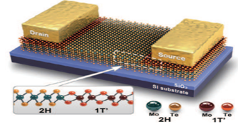
This is the perfect opportunity to employ new, exotic TMD materials. The IBS research team was able to exploit the two versions of MoTe2 and make one 2D crystal that was composed of the semiconducting 2H-MoTe2 and the metallic 1T'-MoTe2. This configuration is superior to using silicon as well as other 2D semiconductor because the boundary where the semiconducting (2H) and metallic (1T') MoTe2 meet to have what’s called am ohmic homojunction. This is a connection that forms at the boundary between two different structural phases in a single material. Despite one MoTe2 state being a semiconductor and one being metallic, the team was able to create an ohmic homojunction between them, making an extremely efficient connection.
To do this, the team started with a piece of their pure 2H-MoTe2 which was several atoms thick. They directed a 1 µm wide laser (a human hair is 17 to 181 µm) at the 2H-MoTe2 which locally heated the sample and changed the affected area into 1T'-MoTe2. With this method, the team was able to create a 2D transistor that utilized an amalgamation of both the semiconducting properties of the 2H-MoTe2 material as well as the high conductivity of the 1T'-MoTe2.
(Above: the 2H-MoTe2 and 1T'-MoTe2 transition line and metal electrodes attached to the 1T'-MoTe2)
This is a clever solution to several problems that have hindered scientists and engineers in the past. By using only one material in the device channel and the metal-semiconductor junction, it is more energy efficient since the joints between the two phases of the MoTe2 are fused seamlessly realizing an ohmic contact at the joints. Because 1T’-MoTe2 is such a good conductor, metal electrodes can be applied to it directly, saving any additional work of finding a way to attach metal leads. This new fabrication technique is a hyper-efficient way of utilizing the available MoTe2 without any wasted or extraneous parts.
When asked about its potential for future use, Professor Heejun Yang of SKKU said, “There are many candidates for 2D semiconductors, but MoTe2 has a band gap of around 1 eV which is similar to silicon’s band gap and it allows an ohmic homojunction at the semiconductor-metal junctions.” This means that MoTe2 can replace silicon without much change in the current voltage configurations used with today’s silicon technologies. The dual-phase MoTe2 transistor looks promising for use in new electronic devices as demand for components increases for materials that are small, light and extremely energy efficient.
- By Daniel Kopperud
Notes for editors
- References Suyeon Cho, Sera Kim, Jung Ho Kim, Jiong Zhao, Jinbong Seok, Dong Hoon Keum, Jaeyoon Baik, Duk-Hyun Choe, K. J. Chang, Kazu Suenaga, Sung Wng Kim, Young Hee Lee, Heejun Yang (2015), Phase patterning for ohmic homojunction contact in MoTe2, Science, DOI: http://dx.doi.org/10.1126/science.aab3175
- Media Contact For further information or to request media assistance, please contact: Mr. Shi Bo Shim, Head of Department of Communications, Institute for Basic Science (+82-42-878-8189; sibo@ibs.re.kr) or Ms. Sunny Kim, Department of Communications, Institute for Basic Science (+82-42-878-8135;Sunnykim@ibs.re.kr)
- About the Institute for Basic Science (IBS) IBS was founded in 2011 by the government of the Republic of Korea with the sole purpose of driving forward the development of basic science in Korea It comprises a total of 50 research centers in all fields of basic science, including mathematics, physics, chemistry, life science, earth science and interdisciplinary science. IBS has launched 25 research centers as of August 2015.There are eight physics, one mathematics, six chemistry, eight life science, and two interdisciplinary research centers.
|
|||
|
|
|||

| Next | |
|---|---|
| before |
- Content Manager
- Communications Team : Kwon Ye Seul 042-878-8237
- Last Update 2023-11-28 14:20
55, Expo-ro, Yuseong-gu, Daejeon, Korea, 34126
Tel. +82-42-878-8114 | Fax. +82-42-878-8079 | E-mail. webmaster@ibs.re.kr
Copyright(c) IBS. All Rights Reserved.
